If you want to build semiconductors at home, it seems like the best place to start might be to find a used scanning electron microscope on eBay. At least that’s how [Peter Bosch] kicked off his electron beam lithography project, and we have to say the results are pretty impressive.
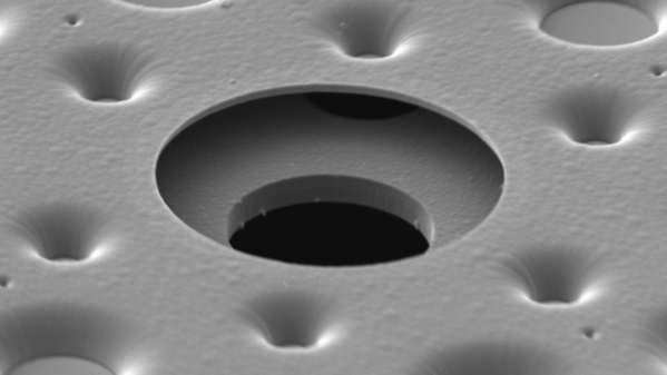
Now, most of the DIY semiconductor efforts we’ve seen start with photolithography, where a pattern is optically projected onto a substrate coated with a photopolymer resist layer so that features can be etched into the surface using various chemical treatments. [Peter]’s method is similar, but with important differences. First, for a resist he chose poly-methyl methacrylate (PMMA), also known as acrylic, dissolved in anisole, an organic substance commonly used in the fragrance industry. The resist solution was spin-coated into a test substrate of aluminized Mylar before going into the chamber of the SEM.
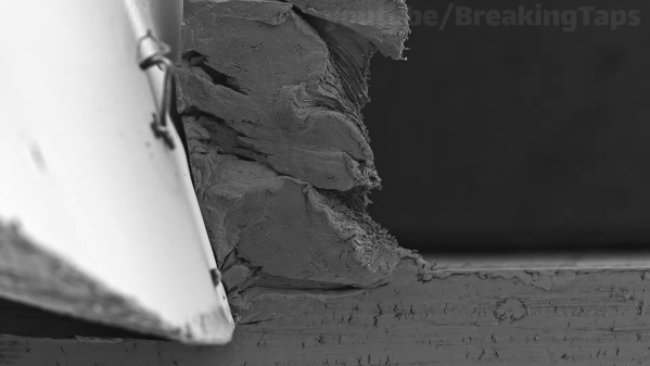
As for the microscope itself, that required a few special modifications of its own. Rather than rastering the beam across his sample and using a pattern mask, [Peter] wanted to draw the pattern onto the resist-covered substrate directly. This required an external deflection modification to the SEM, which we’d love to hear more about. Also, the SEM didn’t support beam blanking, meaning the electron beam would be turned on even while moving across areas that weren’t to be exposed. To get around this, [Peter] slowed down the beam’s movements while exposing areas in the pattern, and sped it up while transitioning to the next feature. It’s a pretty clever hack, and after development and etching with a cocktail of acids, the results were pretty spectacular. Check it out in the video below.
It’s pretty clear that this is all preliminary work, and that there’s much more to come before [Peter] starts etching silicon. He says he’s currently working on a thermal evaporator to deposit thin films, which we’re keen to see. We’ve seen a few sputtering rigs for thin film deposition before, but there are chemical ways to do it, too.
Continue reading “Homebrew Electron Beam Lithography With A Scanning Electron Microscope”