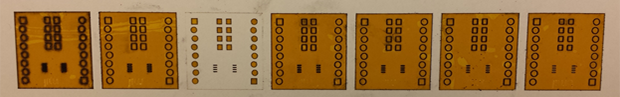
With the proliferation of desktop routers, and a number of easy methods to create PCBs at home, there’s no reason anyone should ever have to buy a pre-made breakout board ever again. The traditional techniques only give you a copper layer, however, and if you want a somewhat more durable PCB, you’ll have figure out some way to create a solder mask on your homebrew PCBs. [Chris] figured Kapton tape would make a reasonable soldermask, and documented the process of creating one with a laser cutter over on the Projects site.
The solder mask itself is cut from a piece of Kapton tape, something that should be found in any reasonably well-stocked tinkerer’s toolbox. The software for [Chris]’ laser cutter, a Universal Laser Systems model, already has a setting for mylar film that came in handy for the Kapton tape,
Of course, getting the correct shapes and dimensions for the laser to cut required a bit of fooling around in Eagle and Corel Draw. The area the laser should cut was taken from the tCream and tStop layers in Eagle with a 1 mil pullback from the edges of the pads. This was exported to an .EPS file, opened in Corel Draw, and turned into a line art drawing for the laser cutter.
The result is a fast and easy solder mask that should be very durable. While it’s probably not as durable as the UV curing paints used in real PCBs, Kapton will be more than sufficient for a few prototypes before spinning a real board.


I picked up some “Pebeo Vitrea 160” heat cured glass paint for making solder masks. If you apply a solid piece of kapton to the PCB and then cut out the pads you want exposed you can pull off the tape leaving kapton over the bare copper pads. You then brush on the paint and toss it in the oven for a few minutes and now you have a long lasting board with colored solder mask!
It would be interesting to test if aplying a few Kilograms of force increases adhesion (through a silicone rubber to ensure maximum pressure distribution.
I like the use of the staggered holes to hold the part in place before soldering. Sparkfun was the first place I saw implement this. I’ve used it a bit since.
It’s good to keep in mind, I’ll try it some time.
Given how cheap & painless fabbed board prototypes are (etched, masked & silk screened), I don’t know if I would make it standard practice to make boards at home. My main exception would be if I needed faster turnaround.
I do make my own solder paste stencils though, from mylar.
Are you guys really doing wave soldering? Because a solder mask is a waste if you are doing it by hand.
totally isn’t if you’re doing hot plate reflow, plus cuts down on the number of bridgeing mistakes for newb.
I’ve been doing similar with plastic sheets and kapton tape, i use the engrave mode and not cut mode. What i want is laser software that can cut rectanges that are wider than longer in X direction, then cuts longer than wider in the Y direction. it’ll vastly improve the cut (at least on all the lasers i’ve used so far)
my notes are here.
http://charliex2.wordpress.com/2013/12/29/making-pcb-stencils-with-cadsoft-eagle-and-moshidraw-2013/
I like your use of “print to PDF.” We are experimenting with different masking tapes to make disposable solder paste stencils. The major advantage is that they stick themselves in place making alignment a snap. The disadvantage is they are single use.
There are two good reasons that we wanted to have a solder mask on our bare boards. The first is the potential for shorting out power plane pours on the top layer with signals when probing around or accidentally dropping something conductive on the board. And as charliex said, it helps prevents bridging problems.
As I have learned from experience, sometimes your proto board are in service much longer then you might intend.
We’ve been doing a similar process in the advanced circuit lab at Metrix Create:Space for about a year. We use a laser cut polyamide/kapton coverlay with a dry adhesive acrylic backing and toss it in the lamination press. Once it is hot pressed, it does not come off. The only real downside is that we have to run the board through the press, which adds time/cost. The upside is that we can apply a permanent mask for laser structured pcbs that don’t require us to revert to wet processing.
If it is single use only, why go through the cumbersome steps of applying/aligning the tape to the board? Just tape it on, align the board with the drawing (==make a outline or a mould for it fixed to the bed) and cut directly on the board. That still leaves you with some nasty picking tape of pads, so the alternative is to switch to engraving mode and paint.
Also: a lasercutter may not make the best cuts as it can melt the sides of your cut (it does that with all plastics). A vinyl cutter can produce sharper cuts as it uses a real knife to cut your material. It still leaves you with picking off the cutouts for he pads though.
There is a product made for commercial use called peelable latex solder mask. I am pretty sure it could be used as a temporary mask whilst making a board mask with spray paint. Although that is not its intended use. A hack? Perhaps. It beats the various schemes I am seeing here though.
If we’re talking about other way of doing a solder mask then I’ll just add that Dynamask 5000 dry film is the nuts. It’s UV curable (like the paints) but it’s laminated on, so far less messy.
CamBam can import Gerber files directly if you can control your laser via GCode. If not, CamBam can them export to DXF. I’ve been using this toolchain to make Mylar stencils for a while on a laser.
Cambam? Laser? Post on the sister site overkilltoday. I mean come on, where’s the hack?
I do exactly the same thing for stencils (with a DC-K40 and a ChrisCircuits.com control board). I think that using gcode to control a laser is unusual though.
We tried if this might be better for solder-paste-stencils. No go.
We tried if this might work as an etch-resist to make PCBs. It seems that might work. The design I tried it on however is too “fine” to make it work, so you need design rules that are a bit more strict than what you get at the cheap prototyping places. TQFP is not going to work. :-(