Building a circuit Manhattan style with small bits of copper and solder is a skill all its own, and building a prototype dead bug style is close to a black art. [Anderson] is taking it to the next level with his volumetric circuits. Not only is he building a free-form circuit that’s also a one-bit ALU, he’s also designing software to make these sort of circuits easy to design and build.
[Anderson] is calling his 3D circuit design software Pyrite, and it does exactly what it says on the tin: creates three-dimensional, grid-aligned physical circuits. Automating the construction of a circuit is not a trivial task, and soldering all these components together even more so.
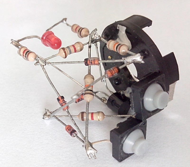
With the first prototype of his software, [Anderson] entered the schematic of a simple one bit ALU. The resulting layout was then carefully pieced together with solder and hot glue. It didn’t work, but that’s only because the schematic was wrong. Designing the software is still an incredible accomplishment, and now that [Anderson] has a rudimentary system of automatically designing free form and dead bug circuits, there are a lot of interesting possibilities. Ever wonder if the point to point wiring found in old radios was the most efficient layout? [Anderson] could probably tell you.
You can check out a few videos of [Anderson]’s work below.


Pyrite used to be a Max object that later became SuperCollider….http://www.audiosynth.com/icmc96paper.html
That’s nothing short of beautiful.
It will be difficult to trump the work of Jim Williams:
Here is an analog living room thermometer:
http://m.eet.com/media/1180890/thermoml.jpg
Wow! That’s beautiful!
Just like my clock ^^
http://www.youtube.com/watch?v=e4SvgMIEc9g
Great work! Now jam that sucker in some clear cast resin!
surely that’s not running off mains AC?! very impressive though!!
Or like mine… :-)
http://www.youtube.com/watch?v=06-RMMxYA1Q
beautiful.
Love it!
I had to turn my sound off about halfway into the second video. The 1980s called and they want their video game soundtrack back! What’s a PBC?
I had to watch more than 500 videos for the hackaday prize. This was one of the best videos in terms of presenting the information, and it had the best soundtrack.
Yeah well ya know that’s just like uh your opinion man
> The 1980s called […]
DID YOU WARNED THEM ABOUT 9/11!!!???
What about ebola, SARS?! Indiana Jones and the Crystal Skulls?!!!
Both 9/11 and the 2014 ebola outbreak are tiny “disasters” in the scale of disasters. How about the 2004 tsunami? It killed nearly a quarter million people. The 2010 eartchquake in Haiti killed 160,000. More people died in the 1988 US heatwave than 9/11 and the 2014 ebola outbreak combined…. So please get some perspective about how serious an event is so your local demagogues can’t control you easily.
Speaking of perspective: http://xkcd.com/875/
and while you’re there: http://xkcd.com/610/
Well, 9/11 was (mis)used to justify the invasion of Iraq, which has killed plenty, and the killing isn’t over yet.
It is interesting that you mention it, because it was actions we took in the 1980s that ultimately lead to 9/11 (See Charlie Wilson’s War). We were warned well in advance too. I can distinctly remember watching a pair of befuddled Afghanis on PBS being interviewed about the destruction of the Buddhas of Bamiyan months before 9/11 just about coming out and telling of the impending attacks in a nationally televised broadcast.
After 9/11 I thought, well, I guess that pair weren’t joking, were they? So we were warned repeatedly. Believe me, the people that run the world today knew. They simply don’t care. You are dirt beneath their feet. If a few thousand of us die they will just use the event to further their own agendas too.
You didn’t like the soundtrack? I did.
Geek culture peer pressure. The struggle is real.
Floating circuits… gee all it needs are ceramic ring spacers and it’s a new discovery of an old circuit like those in variable speed controllers for machine tools from the 1960s.
What’s the trick to soldering 3 wires? When I try, I usually end up loosing the connection to one of the first two when I solder the third.
Heat Sink! Use alligator clips above the area you are soldering to sink the heat away from the previously soldered area.
Of course you are going to “lose” then connection if you are “loosing” them.
Solder them all at the same time.
It is not forbidden to make loop at end of wires to keep them together before soldering
Mechanical fastening is actually one of the rules of soldering. We often lose sight of it because soldering often works even if we don’t do that.
use your teeth.
I’ve often thought that you could make more efficient circuits by pushing them into the third dimension, even in digital applications(especially fast-access memory). What a cool bit of software, and well named too!
That’s what we’ve done by utilizing multi-layered boards for years, along with some of the work also mentioned here. But, bake your noodle on thoughts of ground and power “rails” or “planes” implemented as spheres and thoughts of electronic devices mimicking the very atoms they are made from. ;-)
So, when can I integrate this with my 3d printer? I have been wanting to be able to seemlessly embed electronics into my prints. PCBs and such don’t make much sense but sensors, LEDs and some wireing would be awesome. cool stuff
While I can appreciate such circuitry as art, it really doesn’t have practical value beyond that. If it did, then manufacturers would still be using the “point-to-point” wiring system like they did prior to the introduction of printed circuit boards back in the 1950s.
A real alternative that was 3D (-ish) and practical, and was used by early computer manufacturers (and others) during the 1960s (mainly) was a technique called “cordwood construction”. It allowed for quite high packing density of parts (which is why it was popular for computer construction prior to the invention of the integrated circuit), but it was fairly complex to put together, maintenance was a nightmare, and thermal expansion could cause other issues.
I do seem to recall that Seymour Cray came up with a 3D construction method for some of his later supercomputers (Cray-3?) which allowed for higher density construction (but cooling became more complex).
Another method used (and only used by a few manufacturers – Hitachi is currently the only supplier of it), but isn’t really a 3D construction technique is called “multiwire”; it’s a point-to-point method for wires, where the wires are embedded into a material matrix (usually plastic resin), and can run in any direction. It frees up the issue of PCB trace routing (since the wires can run in any direction freely), and crosstalk is also less (since conductors don’t have to run parallel). But it hasn’t been used much since the 1980s.
Google “printed circuit board”, hit the wikipedia article, and be sure to check out “point-to-point construction” as well. All the history is there, and it is clear that the method of circuit construction espoused by this HAD article is anything but new or innovative. I will say this, though:
That software looks interesting, and the author could do quite well for himself if he modified it to work with tube designs and classic point-to-point chassis-based circuit layout – mainly among the vintage audio crowd. If it had reverse-engineering capability as well (ie – design the p2p then turn it into a schematic) that would be even better. It’s best use would be for those restoring original vintage equipment, as well as building new “vintage” reproductions (think guitar amps, mainly).
I would have thought the reason they don’t do it is because it’s so much cheaper to make a pcb. Pick and Place components onto solder paste and heat.
You’d need little robot arms and soldering irons to automate full on 3D circuit construction.
Although unless you’re limited to non-surface mounted parts, you could probably make a PCB that took up less X and Y space, as well as in the Z axis.
Cheaper? It’s about consistency. Pick-n-place with machine vision does the same job, the same way, many thousands of times.
The method presented here is completely ridiculous and serves no engineering purpose. The circuits are not smaller, would never be consistent when made by two different people or at two different times and could not realistically be troubleshot.
This is art, not some new alternative manufacturing method.
Enjoy it for what it is.
For example:
http://www.manncorp.com/smt/prod-638/pick-and-place-led-mc-ledv4-12.html
15,000 components per hour.
Keep in mind that they components are put on the same way.
I’ve still not used a PCB for my projects (unless as part of a prefab module). I love dead-bugging, though I keep leads only as long as needed, the circuits feel much more compact
An 0201 cased resistor disagrees with you.
When your ground plane steps into the third dimension…
This strikes me as a fun and interesting way to make fun, beautiful, and useful stuff. I wonder how soon before someone builds an Arduino like this?
2011
http://hackaday.com/2011/03/31/pcbs-without-any-substrate/
Mass producing a bunch of tiny jumper-like “micro-breadboards” for the joints could lead to some extremely fun and edumacational kits for kids and noob makers. There’s a lot of possibility here!
“Volumetric circuits” HA! So Anderson has rediscovered what we aptly called “birdsnesting” components on “aeroboard” when circuit developing back in the 1970’s.
I like his ALU intention, this artistry, and his software, but he’s building on a deep history of unconventional circuit layouts, “dead bugs”, “mesa” VHF builds, electronic jewelery, &c. Back when the 2102 1K x 1bit RAM ruled we saw “tower blocks” of eight glued in a stack to convert PCB area into volume.
Not new, but a definite step forwards. 4 Stars.
I remember the ram tower blocks. Did a few of those back in circa 1978-1980….
Straightening out all the pins on them stack them ontop of each other and then soldering the stack to two pieces of veroboard so all pins was in parallel – except for the data_in and data_out pins where you removed the copper strip on the pcb for those two rows.
I can’t find any picture of it on google though…
It could also be done by just stacking the chips as is, and just bend out the two data-pins….
That’s the way I remember it as well-bend out the two pins. I can’t remember what the caveat was (was it chip specific or computer specific?) Anyhoo, haven’t done any stacking in a decade or so, thanks for the memories :)
I love to look at dead bug/ hanging garden/ aeroboard/etc goodies :)
You need a tiny spot welder, then cover the connection with solder to make it very solid.
It is designed to detect and measure the intensity of X-rays emitted by electronic devices during testing and analysis.