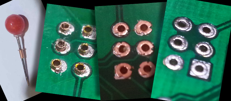
We’ve seen plenty of professional looking, homemade PCBs over the years. But this is the first time we’ve seen such professional vias and through hole plating. Don’t let the green solder mask fool you. This is a homemade PCB.
[Kurt Skauen] started with your standard artwork, followed by etching. He then applied a solder mask that is UV curable. At this point, it’s nothing we haven’t seen done before. After drilling he then adds vias with wire. Again, we’ve seen that before as well. Where it gets interesting is his use of through hole plating rivets. We’ve heard of these micro-sized rivets in the past, but hadn’t seen their use documented as well as [Kurt] has.
Making such a professional looking board at home is practically an art form. One could argue that with today’s cheap, short run PCB fab houses, why bother with trying to do it yourself? Well, perhaps you need a professional looking board to show a client ASAP. Maybe you just hate waiting for your boards to arrive. Or maybe you do it just because you can. Either way, the results [Kurt] achieved are very impressive.


I’ve considered these rivets, however I’ve been told that the forces involved in clamping one can cause microfractures and other PCB deformations. Not sure how reliable would this method be.
We used them in PACE rework school. I don’t think PACE would have us using them if they weren’t a good solution. They definitely knows their stuff.
Agreed. I took the PACE 2m course. The rivets shouldn’t be split along the edges like that. They should be flared by hand with a 45 degree punch, then flattened with a light tap from a flat punch on a small anvil.
As above, I do it because I can, some people argument is that it’s cheaper in hours to get made inpcb house, but my time is being with my hobby, that’s the fun part…if we didn’t do it this way and go buy something, ain’t no fun in that. Build it, make mistakes, learn, get better at building.😁😁😁
Hmmm. I would venture to guess that the soft copper rivets don’t need much force at all. And if you apply it evenly, it shouldn’t be an issue. That and copper traces are super ductile. As someone that had done a lot of home etched, toner-transfer boards, I would say the most trauma is in the ironing of the boards, and drilling. I’ve ripped up a pad by using a dull drill bit before. But I think that’s part of what make home PCB part art and part science.
I’m using a small CNC mill to do the drilling and milling so it minimally affects the PCB integrity. I use another plating process, which is electroplating over a priming layer made by thermal decomposition of copper hypophosphite, but a number of problems with evenness of the plated layer have prevented me from using it for any real boards so far. A proper process using brightener (gelatine + potassium tartrate) could help, but I haven’t yet tried that.
At least you can get the chemicals needed to make the hypophosphite solution where you live! I’m guessing you probably don’t live in the US, where the ‘War on Drugs’ has made several important industrial chemicals impossible for normal people to get! If a person where to go buy some of the chemicals needed to do it, they would auto-magically end up under surveillance, and probably get a visit from some guys driving SUV’s and wearing suits! Some free country we live in! I have wanted to try the thermal decomposition method ever since I heard about it! No messy ink, and with properly drilled holes, you should get really good results.
I have had decent luck activating hole walls with conductive ink, and electroplating through using a copper acetate solution and a bench supply. It takes awhile, but it does work pretty well. The real trick is applying resist after you plate and then not ruining the board when you etch the traces. Dry transfer resist film of decent quality is not easy to find in quantities small enough that it isn’t cost prohibitive. There is always ebay, but the film I have gotten from china leaves a lot to be desired in terms of quality…
Russia, yeah. Instead we banned sulfuric and hydrochloric acid in concentrations of over 10-30% depending on acid (among some other things, thankfully under 20 in total), also ostensibly to prevent drug manufacturing. But in exchange you can mail-order hydrazine (not joking), no questions asked!
I bought resist on ebay and the quality was excellent. I got resolution down to 50um with some experimentation, though of course I can’t etch features that small: http://lab.whitequark.org/notes/2014-06-11/producing-pcbs-using-photolitography/
I use a plating bath recipe from “Printed Circuit Boards: Design, Fabrication, Assembly and Testing. R. S. Khandpur”. You can find it scanned on google books I believe. It’s copper sulphate, H2SO4 and brightener. (How I got sulfuric acid you ask? Battery acid. Nice clean sulfuric acid. Lol, regulation)
Wait…. you can seriously mail order hydrazine????
WTF RUSSIA????
Yeah, seriously. Can I get a link?
Sure! http://xummag.ru/reaktivi_g “Гидразин гидрат кг Ч 658,44р.” approx. $10/kg. I bought chemicals from that supplier in the past, they want your ID and they won’t sell you stuff banned federally. That’s about it.
I also found out that EU doesn’t ban hypophosphite either; DE, FR and UK regulation seems to not list it as far as I could find. Canada does. Seems to be a mainly north american madness.
Agreed that the copper is malleable enough to not need much force at all at that thinness, but then it depends on the riveting gun/tool’s tactile feedback – it’s likely a levered tool and it may be possible to apply too much force if you can’t feel it tighten. There’s also risk of the rivet buckling inside the hole (and stretching the PCB) if using a clamp like the OP
Always been somewhat leery of PCB rivets, myself… If nothing else, they’re not particularly cheap.
But it occurs to me, they could be used on single-sided boards/breadboards, etc. Especially when using components/connectors which could/do torque the pads off the underside. Handy.
I’ve used the rivets before, they work pretty well, but its time consuming and you limit yourself to certain hole sizes. For example, for my software its not unusual to find footprints with 31 mil holes, 34 mil holes, 38 mil holes and 40 mil holes. One may have to modify the padstack so all are say, 34 mils, which all the components will fit into easily and this saves time by only using one type of rivet. Otherwise, having all sizes and trying to figure out which one goes where is a pita.
I used them a lot in the last years. I would’nt say that they aren’t cheap. 0.02cents a piece is not to expensive
As in $0.02 each or 0.02 cents as in you need to buy 50 to make up one cent?
I remember using these back in the late 1980s at a company I was working for at the time. I don’t recall ever having any trouble from them, and they were very quick and easy to fit.
We use these rivets in my place of work. They work OK although you can only do one at a time and you get the occasional one that doesnt qquite have a great connection so it needs a blob of solder. I’ve had better experience with just pressing pieces of wire into holes.
Ok, the rivets are one thing … but … but … this guy is just NUTS!
His PCBs are art. And he’s doing it all with the same el-cheapo-DIY-tools we all ourselves are using (except for the vacuum UV box). And he’s doing it so much better.
I torn between disbelief, admiration and envy. This guy is nuts.
I use these same method for my boards and its really handy but not exactly cheap as others have said. IF your in Europe these cost ~0.03/qty 1k but when your getting them from ebay their ~13/qty 200 and much lower quality. I use them only when in a pinch where I need a double sided component pad. For everything else I solder the empty hole and push a wire through, snip it both sides and smoosh with a vice.
Wow…… that is some special kind of patience. Does he say how long it takes ?
I think i should come back to making pcbs at home. getting ones for cheap from china is great…. but it does kill the buzz of a hobby project during the 1 month of wait time…
Go with DF Robot and select their low cost DHL shipping (price seems to vary, but less than $10 shipping last time I ordered). You will have boards in about a week, unless it’s Chinese new year.
Yep, i actually remembered i did that twice already. About 7-8 days from submit till pcbs in hand for $26. No edit on the comments though.
If you are going from paper to schematic to PCB to proof of concept to prototype in one day verses several days, cost really isn’t as much a factor as showing what can be done in such a short time. I’ve found it cheaper and promotional to do so….
Press in ferrules and rivets like this have been available for decades. WE used to do that when we made out boards in college during the late 80’s.
This is not new, and you dont need the flanges. straight copper ferrules work great and the solder flows in and locks them in place easily.
Now home wave soldering…. That will highly impress me.
This isn’t even technically Plating and is old tech from the 70’s, 80’s, and early 90’s. I too am not impressed
This process was taught in the U.S. Navy (2M) Micro-miniature repair schools in the early 1990’s. It was a tough class, about 1.5 months. Eyelets, which is what they are called, were used in board repair to replace the through-hole. It is very tedious work and you have to flair out the back, like shown here, and then tap them down. It takes a lot of patience, if done wrong the component leads will not go through. This looks like a great job and the board looks awesome.
The main reason for doing pcb’s yourself these days is for making evil, untraceable, things, like IEDs and pressure cooker devices. Look suspiciously at anyone doing their own boards or buying the supplies.
Rivets look like crap and will perform as well in temp cycling. Then there’s the chemical disposal problem – everyone pours it down the sink. To save zero money of you factor boards, shipping, chemicals and time.
There is no legitimate reason to do your own pcb’s anymore. Even the argument of immediacy is BS.
It’s not so much that you’re horribly misinformed. It’s that you’re so misinformed as to think IEDs need a PCB.
seriously. everybody knows those are all dead-bugged/ptp. except maybe in the movies where a pcb adds a sense of legitimacy to non-technical viewers.
Don’t forget the blinking LED and the little piezo beeper. They don’t work without that… just ask anyone in Hollywood.
What a total load of crap. Making your own boards is just like any other hobby. It’s an enjoyable way to waste your time.
It is enjoyable indeed. Also, the ability to produce our own 1 or 2 sided prototype boards whenever we want, and whenever we feel like it … is pretty good actually.
That’s some Grade-A Premium BS right there. I derive happiness in the challenge of making my own PCB’s for my varied hobbies and electronic needs. I’m not going to allow fearmongering authoritarians and their mindless lackeys take that away from me.
+1
I couldn’t agree more. I have all of my IED boards done by a PCB fab house. Bombing is one thing, but pouring chemicals down the drain is just inappropriate. I’ve found that the rivets hold up just fine, but I only heat cycle them once for a very short duration.
*knock knock*
“Sir, do you have a few moments to answer some questions?”
“Oh of course not, why would you need a lawyer?”
You don’t get to see a lawyer these days. On the other hand, you might win a trip and accommodation south of the border which should be much nicer than the freezing stuff outside. Even comes with 24/7 securities and personal trainers.
At first I thought you were joking, because it seemed like you went on to make a serious comment, but at the end you made it quite clear that you are in fact ignorant as hell…
People like you are why the first pictures I circulate of any new project have filenames like notabomb_01.jpg (Because, really, what terrorist would take pictures of a bomb and then go around showing everyone and saying it isn’t a bomb? Am I right? My logic is flawless.)
And what would you do for minimum cost in modest scale production as a start-up? Do a high volume deal with a professional PCB maker? Or try to make your own efficiently. Not all basement entrepreneurial types are bombers and terrorists. At least… I don’t think so. Check with me later. Lol
I often see a HaD post and think “Wow – that’s exactly what I need right now”. Then realise I’ve seen it already because you just read the same blogs and forums as I do – Eevblog in this case. I’m about to etch a board that’ll use these rivets (0.6mm ones for vias). I use similar processes and I’m slowly getting there on the quality.
Definitely a great write up from Kurt. All those people who think people are interested in how you do toner transfer for your Arduino shields, take note. *This* is how it should be done.
And yes – it is quicker, easier and higher quality to get your boards made professionally in China for peanuts. Some of us enjoy seeing what we can create ourselves.
It is nicely done. The extra height vs plate through vias do not work too well for low profile SMT parts. I have always position them in accessible locations outside of foot print which is a pain in routing. I try to keep the via count below 20, so wires are not a big deal.
I read that someone was using regular copper wires as rivet and flatten them with a hammer. That would work a bit better for thin parts like TQFP. I bought some 0.4mm twist bits from China recently and as it would be a snug fit for #26 solid wire. If the hole is too big, the excess wire would ended up bent inside instead of being flatten at the top. I have been too distracted to try them out. :(
I once worked on a dead Motorola solid state 150 Mhz amplifier. Several of the large through hole eyelets had broken their solder connection, suspect due to the different thermal expansion properties of copper and fiberglass.
I use rivets all the time. I don’t bother smooshing them, though. Just solder in place and done. Sometimes I trim the backside with flush cutters. Mostly not.
1.0 mm diameters have a 0.8mm interior, which is about right. Buy yourself a nice 1.0mm drill bit and it feels really pro.
“…cheap, short run PCB fab houses…” Maybe I have been under a rock for the past ten years, or maybe my definition of “cheap” differs from everyone else, but… I have yet to come across a company that can manufacture a single PCB cheaper, or even anywhere near as cheaply, as I can etch one at home. I have used the ferric chloride / toner method for decades and have recently started just dremeling the copper away from the traces – granted it’s not “pretty” but I have always been more “function over form” than the other way around. Even looking at a small desktop CNC machine, I think I could jusify it’s cost in the saving of having several PCBs “professionally” done.
On topic, though.. I like the use of the rivets. Beats just soldering a piece of wire through a hole or soldering a component on both sides of the board!
you can get 10 boards made for something like $15-$20, even if you ignore that that is proper two-layer boards with vias and solder mask, that’s hard if not impossible to beat to beat at home. Bare PCB, chemicals, drillbits, etc. cost money.
A desktop cnc definitely doesn’t make sense money wise, you’ll spend more on engraving bits than it would cost to
get boards made
I would be extremely greatful if you would tell me where I can get 10 boards for $15 to $20, because everywhere I have looked wanted a LOT more than that!
My problem is that I don’t tend to need 10 boards. Since my projects are usually not duplicated, I typically only need one copy of any board. Ironic for a professional technician with 25+ years experience in consumer electronics repair, but I suppose I would be considered a hobbiest when it comes to PCB design. I guess I am still waiting on that one great idea to hit :)
As for the CNC, you’re probably right, but it’ll be fun nevertheless :D
I used Elecrow bazaar for my HaD contest project. I pushed the board to their recommended geometries and they delivered.
Project page: http://hackaday.io/project/1347-fpga-computereval-board (following URL are relative from project page)
Order detail on my log: log/5358-pcb-is-on-order
$11.90 is 10 pieces of 10cm x 10cm PCB with via Hong Kong post, it comes to $21.57 total
PCB Files sent: July 22, PCB received in Canada on Aug 07
Good communication as indicated by their email.
Large board scans here: log/6562-blank-pcb-scans-large-files
This board cannot be done with milling nor home PCB fab.
I’ve used these guys a few times: http://www.seeedstudio.com/service/index.php?r=pcb
I can’t remember the price the last time, but once was less than $15.25, including shipping, for 10 5cm x 5cm boards. It took a few weeks between order and delivery, but I also remember there being mention of a holiday. Fiddle with those settings, sometimes you can get an upgrade (quantity, stencil layers, whatnot) for free…
Also, they’ve been very helpful when weird things have appeared in my Gerbers. I can’t believe they were able to spend so much time on them for that price.
I haven’t used any of them but I’ve seen many do, but just to name a few
http://dirtypcbs.com/index.php
http://www.seeedstudio.com/service/index.php?r=pcb
http://smart-prototyping.com/PCB-Prototyping.html
https://oshpark.com/
“Maybe I have been under a rock for the past ten years…” I, too, crawled out of said rock, just recently… Within about the last ten years is about exactly when “cheap, short run PCB fab houses” seem to have popped up. I remember being ecstatic to find the 3*$33 deal, and even more-so when they bumped it up to 4*$33. But $99 for three PCBs is only justifiable (to me), these days, if they’re *huge*, you have enough money to *be able to* support local, or you need them ASAP.
But, more importantly… “have recently started just dremeling the copper away from the traces”… Someone once told me something along the lines of: “Back in Soviet Russia, we cut traces in copper-clad with a razor-blade.” I tried it once, long after getting professional PCBs made somewhat regularly, and it worked *amazingly* well, especially for big boards with few/large traces (e.g. a power-supply). Just peel it up. No Mess. Wondrous. And lots of space for minor-changes.
Seriously…. Stop writing articles about how home etched PCBs are somehow just than professional boards. You don’t need to make stuff up. You don’t have to add extra fluff to the articles. Just say what it is. Making boards in your garage is purely a hobby, like stamp collecting. Is it skilled and a bit artistic? Maybe. Is it a good professional use of your time? Not really.
If I contracted a client to make a PCB for my company and they showed up with something they etched in their garage, they would be fired immediately. I don’t care what it looks like or how many tricks they played with tiny rivets or packing tape, you don’t do that kind of stuff in a real business. If you are making a product for sale, you don’t screw around and try to hack stuff together in your garage. You treat it like a business. Even if it works, you are going to need to re-qualify the product after the real professional boards get made since they are going to be using completely different processes. The qualifying time is going to be WAY more expensive than what it would take to just get some damn boards made professionally on the first go. If you need boards NOW!!!!, Advanced circuits has SAME DAY board service. Is it expensive? Yes it is. Is that expense something you pay for when developing products quickly for sale? Sometimes yes.
If you had stopped your article at “This is a novel way to make double sided boards in your garage.” And not added any of the other junk about how you can make “professional vias and plated holes” then you would have been fine. There is nothing professional about this. Hobby. Stamp collecting. That’s it.
Do you even know what site you’re on? This is by hobbyists for hobbyists. No one cares what you and your BS business thinks. Sure you don’t even know what website you’re on FFS.
I agree with you!! That is my whole point!!!! Make it about the hobby.. You don’t have to throw in the “Well, perhaps you need a professional looking board to show a client ASAP.” That is just stupid. The mini rivets things is a cool idea. I like it. I like the packing tape idea too. But lets not pretend like that’s how real business work. You don’t go have purchasing order a new roll of packing tape and ferric chloride every time you need 100 more boards, and you don’t go order mini rivets when you need to go to show a board to a customer. Just stop at “these are interesting methods to make one board in your garage for yourself if you really want to do that”.
Laying out a board for one off or prototype purposes the diy method is great. Design revisions can be made same day and refinement of the pcb justifies the time invested. Paying for a batch of pcbs which are prototypes to me is a waste of resources when revisions inevitably get made. When I’m ready for a production run then the pcb house gets gerbers. Doing this for 20 years this way and not going to change regardless of pcb fab house cost. The rivets are a good solution to the tough diy challenge of vias.
Time is better spend getting the layout of a professionally made board right the first time, than rushing to mess with chemical to get a sketchy prototype that needs several revisions
I agree with the Fonz. Two thumbs up! Heyyyyy!
If you’ve never had to make revisions to something– if for no other reason than simply to account for discrepancies between how things worked on paper and in reality –it’s rather hard to believe you’ve ever designed anything.
I do it for a living, revisions should be the odd exception not the norm and it is if you do things right. When time is money and a board is easily several $100s in parts alone you don’t just throw together half assed prototypes
AC an fonz obviously don’t have to deal with customers who like to change the goalposts, or alternative component choices just for the sake of trying them out. Same day prototype turnaround cannot be beaten for time critical projects. I have prototypes still in use 12 years after leaving the lab!
I been using these for quite a while for through hole vias, i buy mine from UK (im UK bassed) from MEGA UK – http://www.megauk.com/through_hole_rivets.php at £24 for 1000.
I use a drill punch to splay the ends out and then a light hammer to flatten them. Then use solder/plating to connect them and make the board look sweet!
Sadly this was something i was doing before i had my Flickr account so no pics… :(
I use the 1.0mm through holes when i am soldering a through hole component too and 0.6mm for standard vias.
None of you fuckers said a word about sending your PCB design anywhere. What the hell, they can just photocopy it anyway when you go to market. Not an issue at all. Send them source code/hex too so they can help you out.
Don’t call that plating – it is not. Notify me when you get to real plating, that will be interesting. Vias that hold well when soldering or desoldering – for that the rivet method should be good, but it’s time consuming anyway.
And by the way, don’t forget some kynar for some hot fixes when all of your 20 boards don’t work. Or 2000. I have seen that shit in few computers, I bet they were in hurry
I’m inclined to agree that, yes, professional PCBs are the way to go–most of the time.
Heck, after grad school, I never ordered another board without a solder mask and silkscreen.
Q: So why would we even consider making DIY PCBs?
A: To make transparent PCBs that are 36×48 inches (91x122cm).
The widest “giant” PCBs I found anyone willing to professionally fab is 24 inches (61cm).
And those are neither quick turn nor affordable.
So I am carefully doing my homework before getting into DIY PCBs.
And you all have been great!
For us, etching isn’t the problem. It is the 6,000 drill hits.
And replacing drills before they wear out or break.
And restarting the drill script where things went wrong.
And verifying the final product.
And the joys of throwing away $200 worth of materials each time we screw up.
Even automated assembly is not a panacea for large-scale prototyping.
Earlier in this project we hired an assembly house with a pick-and-place machine.
They machine-placed 90% of the parts before noticing the machine couldn’t reach one edge.
And they shipped us back most of a reel’s worth of SMT transistors loose in a plastic bag.
Apparently this lossage was standard operating procedure when they verified a PnP script.
Lesson learned: hand-placing 2,000 components on a prototype PCB might really make sense.
Thank you to all who posted!
Speed up your riveting and improve the result by modifying an automatic punch tool:
https://www.johny.dk/Print_gb/Nitteværktøj.html
Corrected previous link to the rivet tool:
https://www.johny.dk/Print_gb/Rivet%20tool.html