Remember when PCBs were green and square? That’s the easy default, but most will agree that when you’re going to show off your boards instead of hiding them in a case, it’s worth extra effort to make them beautiful. We’re in a renaissance of circuit board design and the amount of effort being poured into great looking boards is incredible. The good news is that this project proves you don’t have to go nuts to achieve great results. This stars, moons, and planets badge looks superb using just two technical tricks: exposed (plated) copper and non-rectangular board outline.
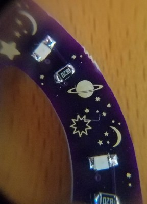 Don’t take that the wrong way, there’s still a lot of creativity that [Steve] over at Big Mess o’ Wires used to make it look this great. The key element here is that copper and solder mask placements have extremely fine pitch. After placing the LEDs and resistors there’s a lot of blank space which was filled with what you might see in the night sky through your telescope. What caught our eye about this badge is the fidelity of the ringed planet.
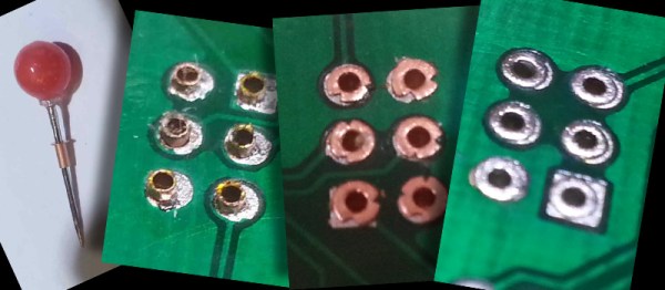
The white ink of silk screen is often spotty and jagged at the edges. But this copper with ENIG (gold) plating is crisp through the curves and with razor-sharp tolerance. It’s shown here taken under 10x magnification and still holds up. This is a trick to keep under your belt — if you have ground pours it’s easy to spice up the look of your boards just by adding negative-space art in the solder mask!
[Steve] mentions the board outline is technically not a circle but “a many-sided polygon” due to quirks of Eagle. You could have fooled us! We do like how he carried the circle’s edges through the bulk of the board using silk screen. If you’re looking for tips on board outline and using multiple layers of art in Eagle, [Brian Benchoff] published a fabulous How to do PCB art in Eagle article. Of course, he’s gone deeper than what the board houses offer by grabbing his own pad printing equipment and adding color to white solder mask.
The art was the jumping off point for featuring this badge, but [Steve] is known for his technical dives and this one is no different. He’s done a great job of recounting everything that popped up while designing the circuit, from LED color choice to coin cell internal resistance and PWM to low-power AVR tricks.