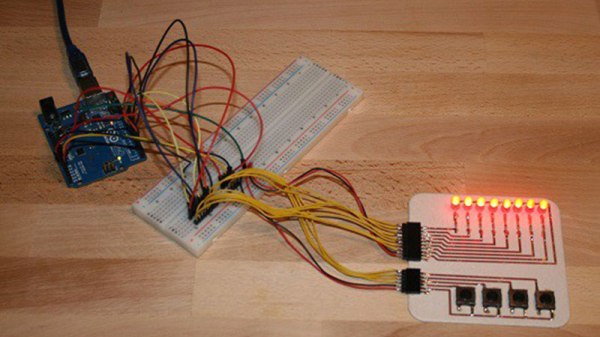
[LudwigLabs] is creating PCBs using copper foil and a cutting plotter (vinyl cutter). In this approach, it’s an additive process where instead of removing copper from a copper-clad board, the traces are cut out of copper foil and transferred to a solid backing surface (cardboard, fiberglass, etc.).
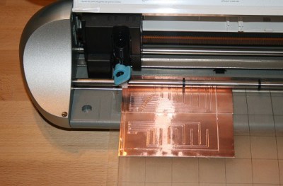 While similar to the use of copper tape laid out by hand, as covered by us last year, the big advantage of using a cutting plotter is that it allows one to create much more complicated traces similar to those you would expect to see on a factory-made PCB. Since cutting plotters translate a 2D design into very precise movements of the cutting blade, this allows for sharp angles and significantly thinner traces, allows designs from EDA software like KiCad or Altium to be quickly translated to physical boards.
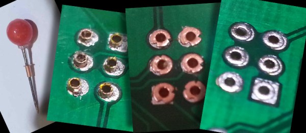
Enterprising hackers might consider the possibility of using this approach to make two-sided, and even multi-layered boards. The copper is produced separately from the substrate which opens up the potential for using uncommon materials like glass or paper to host the circuits. The main limitations are the transferring of (very delicate) copper structures and creating vias without damaging the traces.
As a comparison with traditional PCB fab processes, the photo exposure and etching (or laser exposure and etching) process requires the creation of masks, UV exposing a board, etching, cleaning and so on. The simplicity of copper foil traces has led to many experimenting with this approach. Would you want to use this additive process, or are there refinements or alterations you would make?