To err is human. And to order the wrong component foot print is just part of engineering. It happens to us all; You’re working hard to finish a design, you have PCBs on the way and you’re putting in your order into your favorite parts supplier. It’s late, and you’re tired. You hit submit, and breathe a sigh of relief. Little do you know that in about a week when everything arrives, that you’ll have ordered the wrong component package for your design.
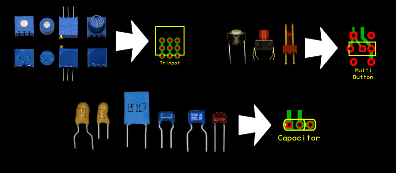
Well, fear not. [David Cook] has a solution that could save your bacon. He shows you how to design multiple footprints into your board to avoid the most common mistakes such as voltage regulators with different pin-outs than expected. Other uses for the trick include, common trim pots with different pin spacing and a layout for decoupling caps that will fit both a 0.1″ and 0.2″ footprints.
We’ll file this under the “Why Didn’t I Think of That” category. It’s a super simple hack, but that’s what we love about it. We could see this being very handy for people who often scavenge parts. Also, for makers that sell just a bare PCBs (without parts) to those that want just a board. No, it won’t save you if your need an SMD and you mistakenly ordered a dip, but at the end of the day, it’s a nice trick to keep up your sleeve. You might never know when you’ll need it.


Extra Credits for those sharing their libs.
Also: Nice other tricks on his page.
Not a bad idea, but seems like it would add up to be a huge waste of board space, usually for me, space is a premium.
I have been caught out with footprints before, but its fairly rare. One thing I’ve learnt is when creating a new part, create a footprint especially just for that part, that way mistakes are minimised by avoiding reusing similar footprints.
I had a similar issue when designing my first PCB. The board needed to fit inside a 3/4″ OD hula hoop which made space a premium (for the bulky parts I selected). I was excited when I received the boards, but very disappointed once I’d soldered it all up as things weren’t working.
Long story short, I had not been careful enough in distinguishing common anode vs. common cathode leds. It was a long week waiting for the replacements, but in the second revision I added an extra pad to accommodate both types.
There are definitely scenarios where planning for alternatives to a particular part can be useful.
I’ve observed this in a variety of electronic junk I’ve disassembled. Sometimes the footprints are one-inside-the-other to save on space just like David Cook shows. I.e. sometimes a SMD component’s footprint smaller, inside the TH one. I think designers do this also because they don’t know for sure what component will be available (or arrive first on the UPS truck) when the boards come in.
I think the waste of space would only be “huge” on a huge board with very tightly packed components. If that’s the case, some other questions should be asked like “are we building with discrete components where it should be more integrated stuff” or “wait a minute maybe if the board is this huge and tightly packed we should be more sure of our supply chain” etc.
It’s always interesting when I find boards with unpopulated or extra footprints. Sometimes you can tell from the labels that the same PCB was used for two totally different devices.
I believe it’s more about PCB re-use as it’s cheaper/simpler to be able to use the same board again for a ‘lesser’ version of the same thing, such as by swapping out beefy regulators for smaller SMT ones. While a lot of manufacturers do offer lower rated devices in the same packaging (ICs/FPGAs for example), sometimes you have to change manufacturer to get the best cost/’fit’ option.
That doesn’t rule out the them hedging their bets because of intermittent supply (would like part A because it’s cheap but sometimes have to fit part B because it’s at least available) but it’s usually for larger runs of the board where having entirely different PCBs can create confusion or extra costing (have to have stock both variants).
Just yesterday I routed in some extra via’s in a board for different sizes of film caps. However in the end finishing a board is packing the right components on there; on a home budget I want compact homebrew boards. I do like the idea for prototypes, or for a project to share that is a bit more flexible to different home builders. For parts like switches and pots it makes sense, it looks like he’s got them and then some nice PCB design tips.
It’s not really a new idea. I’ve been using similar techniques for my mcdox keyboard project. It uses a single footprint to support CherryMX and Matias/ALPS mechanical keyboard switches, thru-hole or SMD diodes, and thru-hole or SMD LEDs, and is all double sided.
For example: https://github.com/DavidMcEwan/fp-lib-dmcewan/blob/master/dmcewan.pretty/alpsmx.kicad_mod
Actually, I DID think of that.
An issue I had and not covered here is having parts with leads that are too fat for the holes.
I thought he did cover that to some extent.
I have done this for a very long time and I think that it is a waste of time, in general. It only works for TH parts, exactly the ones that you can bend the pins of and then plug in, in the end.
I have however found other cases that are more useful: don’t know what a SMD res/cap is perfect for the final? it’s better to put a TH footprint on top of the SMD one and use a socket so you can change a TH resistor a few times before the final one.
I would say that for hobby, its a better discipline to try and buy all parts of the same kind, like always buy the same type of trimmer.
This is stupid because it is not new! I did this already when I invented the atomic bomb in 1820. /s
There, I got you all beat now.
Every article, there just HAS to be at least one.
Sorry, Bogdan. That was not meant to be a direct reply to you. It was general commentary.
I have seen circuits with pads for SMT part substitution, All my experience is in automotive stuff so perhaps this is particular to this industry as most manufacturers will fit whatevers in the parts bin to do the job and substitutions are commonplace.
If you do that Murphy’s laws will apply. The part with the wrong package will be the one you did not put alternative footprints for.
Elektor / Elektuur used to do this quite regular for some parts back in the 70’s and 80’s which are frequently made in differnt size’s. Especially for large elco’s and print transformers which come in lots of different footprints.
Another tip is to spread around some wild via’s and/or smd pads on un-used board space, especially for prototype’s. Even a few vias with odd spacing in between can help a lot when you have to make some small mods, add a transistor, solder a wire for a robust test point, etc.
Here’s how I handle it: I order all my parts and CHECK THEM for fit – BEFORE – sending files off for my boards to get made!
CRAZY! right?
And if I get sent the wrong part on future builds for board that I have already, I HAVE THE RIGHT FREAKING PARTS SENT AGAIN. Most if not all of the big part houses will work with you if you call and complain. If not, you need to stop doing business with them.
I don’t understand, at this lowly, electronics hobby level why the hell anyone couldn’t order their parts and check them against a 1:1 print of your board layout first. If you don’t, YOU are a FAILURE.
And then when your part goes into production, you know there are not going to be any substitutions that will need to be made later if a supplier or particular component drops off the map.
That would add weeks to the development of any of my boards. So far I’ve only been bitten once – I thought I ordered a SOIC16, but I got a TSSOP16, so I had to reorder the parts.
> And if I get sent the wrong part on future builds for board that I have already, I HAVE THE RIGHT FREAKING PARTS SENT AGAIN.
But how long will this take? Some people do not have time to reorder. This is not mainly for accommodating parts ordered by mistake, rather to have more flexibility in the parts that you can use.
Me too, just order all part and check them on paper with printed pcb image with 1:1 scale.
Is curious how many people there make a lot of pcb with long time period so they need alternative footprint for far future.
It is not always “ordered the wrong part” that bites you. In about 10 years as a day-job EE I’ve been burned more than a few times by parts on a production design suddenly going non-buyable for some reason or other. Besides actual EOL’ed parts (which the vendor “usually” discloses in advance), they can decide they’re no longer selling in modest / subreel volumes, or a bigger fish specs their part in a hot-selling product and suddenly all distributors are out of stock with 20+ week leadtimes.
For SMT production designs, if space permits and a given part is sole-source I now usually design in multiple footprints and/or a hybrid footprint that will take multiple vendors’ similar parts. In many cases one footprint can be placed inside another,so this can be done “for free” spacewise.
I’m in the process of desiging a diy-friendly integration motherboard of sorts (a baseboard to hold modules that are already buyable and should just plugin and work). I plan to have some hole patterns setup for some modules that I own or have in mind, but for all others, a ‘catch-all’ set of .1 grid proto holes nearby will do. you can then solder in sockets or whatever to adapt YOUR modules. for me, that’s a way I’d like to have diy’s and so I want to try this on the next project I create.
and, anywhere you have spare board space, why not make it a grid of ‘proto holes’ just in case someone wants to add something in? why not? if you can, try to. those of us who like to get boards and ‘extend them’ love to see stuff like this.
One thing he didn’t cover, although it is similar to the Voltage Regulator footprint, is the layout on my DMM for hFE testing,
It has the transistor sockets laid out in EBCE fashion to accommodate the two most common pinouts.
I do this all the time for bypass caps. Simple, doesn’t take much extra room and it allows you to use whatever source is convenient.
I’ve created custom patterns to allow straight or right angle BNC jacks, tactile switches and USB connectors. A little forethought allows a lot of flexibility in how a board is used.
This is a cardinal rule for me (another is to always doing a DRC before ordering the board): Always order new parts *first* and test-fit them on a paper printout of the board. This rule, and a little patience, has saved me hundreds of dollars.
I’ve done the paper printout test many times. Printing on cardstock is a good way to test for the board fitting in enclosures.
The only time I didn’t bother with the paper test was the time it turned out wrong (parallel port socket not close enough to the edge meaning the cable couldn’t be plugged in. Fortunately I was able to desolder the socket and cut off the edge of the PCB – lucky there were no traces there!)
As for the multi-footprint idea, I’ve been doing that for ages after seeing it in commercial designs.
I have integrated 4 different power supplies into products before because of scares over getting the supply for the volume required
Also i almost always for products built to a cost include footprints for non-telenium caps (mostly thru hole for size constraints) as there are sometimes sudden price spikes on telinies in quantity
Its also a good practice in high cost units to include footprints for parts that might not be available for repair (or easy to get in less than a production quantity) or dip packages as drop in replacements where space is available
But if anyone asks you to include 2 different 42 pin display connectors on a 2 practical layer board ask for a bonus XP … or make an adapter XD
I’ve seen this quite often in consumer electronics from cheap toys to expensive computer components. One example, on some Adaptech SCSI controllers they’d put a SMD footprint inside a DIP footprint for the BIOS, and also design it to use either a one time PROM or mask ROM, an EPROM or EEPROM, as well as different sizes. Thus one board could be used for a less expensive model with a soldered on, non-flashable BIOS, a more expensive model with an EEPROM or removable chip for updates and a Macintosh version that needed a higher capacity BIOS chip.
Some times they’d just program the smaller PC BIOS to the larger chip used on the Mac version and money could be saved by buying the PC version then flashing the Mac firmware. Another trick was removing an SMT PC firmware chip then soldering in the larger DIP socket to install Mac firmware.
Multi-footprints get used on cheap products because the manufacturer wants to use whatever parts are the lowest price *right now*. If that changes in the middle of production when more parts need ordered, all that needs done is to make sure what’s purchased will fit one set of holes or pads instead of spending more money and time redesigning and manufacturing the boards then scrapping the previous design or storing them and waiting on good prices for the components that fit.
The Arduino Leonardo does with the Atmega32u4. They have both TQFP and QFN. The QFN fits inside the TQFP. Great since the TQFP Atmega32u4 can be in short supply.