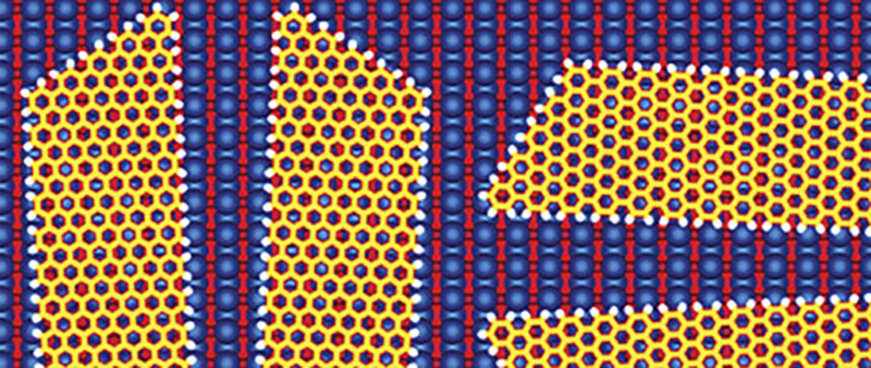
No modern technology has been met with more hype than graphene. These single-layer sheets of carbon promise everything from incredibly efficient power grids to more advanced electronics to literal elevators to space. Until now, though, researchers have yet to produce graphene sheets or ribbons in a reliable way. Researchers at the University of Wisconsin at Madison and the US Department of Energy Argonne National Laboratory have done just that, growing graphene nanoribbons on the surface of a germanium crystal.
By using a germanium crystal as a substrate, the researchers have found a directionality to the way these graphene nanoribbons form. This has been a problem for researchers experimenting with graphene microelectronics in the past; labs experimenting with making transistors out of carbon nanotubes found growth is highly unpredictable. The controlled growth of graphene nanoribbons opens the door to more precise fabrication, something that is necessary for microelectronics fabrication.
Synthesis of nanoribbons this small have not been possible before. Because germanium itself is a semiconductor – and was used for the first transistor – this discovery may pave the way for the creation of graphene-based circuits grown using the same semiconductor fabrication processes used today.


Jeri Ellsworth builds transistors at home:
https://www.youtube.com/watch?v=vmotkjMSKnI
https://www.youtube.com/watch?v=-Qph8BNrnLY
THAT’S FREAKIN COOL!!!!!!!
Damn, Wisconsin is on fire this week.
http://www.reuters.com/article/2015/10/13/apple-wisconsin-patent-idUSL1N12D2D320151013
Damn! I dont think ive ever heard of Apple losing an IP case like this before!
I’d love to know what the patent-able IP is. The linked article is clearly intended for the layperson and only tells us that it’s a “patent for improving chip efficiency”. Is it a semiconductor-process or an architecture thing or something else?
Found an older article, looks to be an architecture thing. Resolving data dependencies and skipping duplicate memory reads in a multi-processor environment.
http://www.patentlyapple.com/patently-apple/2014/02/apples-a7-processor-targeted-in-new-patent-lawsuit.html
Good job Wisconsin. In the meantime if you want to buy some graphen on either Cu, PET, SiC, sauté or in a sauce from Nano Carbon.
Disclaimer: I have no relationship with Nano Carbon other than that I live in the same city they operate.
“Synthesis of nanoribbons this small have not been possible before”
You might be exaggerating. Quote from the abstract “scalable synthesis of nanoribbons with this precision directly on insulating or semiconducting substrates has not been possible”. This is not about farming graphene, it’s about using them in the chips.
Glad to see this is being developed, but it will of course still be years before the average person sees anything with it in it. And naturally development of actual uses for this will be near completely cock blocked by IP legalities.
Interesting!
I agree this is cool, but you could buy graphene on silicon carbide since at least a couple of years! http://graphensic.com/graphene-material/