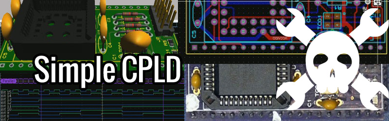
A Complex Programmable Logic Device (CPLD) is a great piece of hardware to have in your repertoire. As its name implies, you can program these chips to serve the logic functions you need. This might be replacing an obsolete chip, or maybe just a way to learn and try different techniques. What better way to learn than to get your hands on a CPLD and give it a try?
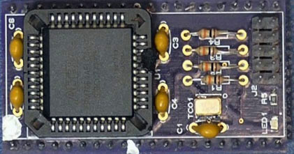
I created a CPLD module with the intent of being able to plug it into lots of things including solderless breadboards, but I screwed up. It seems that the plugin space available on a solderless breadboard is 1.1”, I had made the footprint 1” wide leaving no room for a row of wires on both sides. Duh.
But let me back up and show more about what I’m doing , I wanted to make a programmable piece of logic that could be built as a kit one could easily solder at home, could be programmed in-circuit, and could work at 3.3 or 5 volts.
 To implement an easily solderable kit I went with an older CPLD part that also has 3.3v and 5v versions that will maintain its programming regardless of power. The logic itself is a CPLD IC from the Altera Max family with two versions that fit the board with either 32 or 64 macrocells. A macrocell is the basic logic building block and it is programmed with logic “terms” and then interconnected to other macrocells through a programmable interconnect.
Project Files
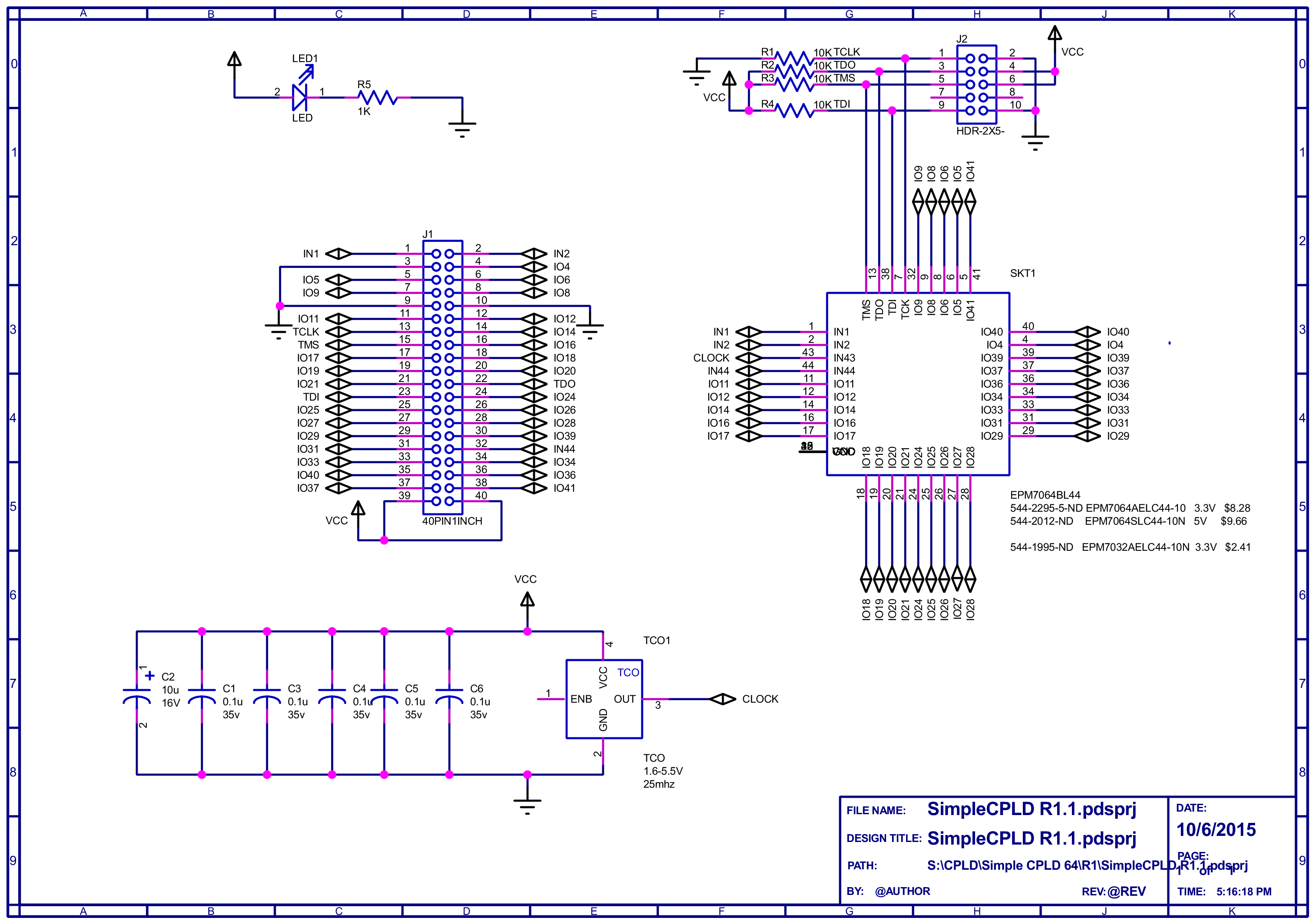 Looking at the schematic you can tell there isn’t much to it: basically the CPLD, the circuit for In Circuit Programming and an oscillator to drive the logic in the CPLD.
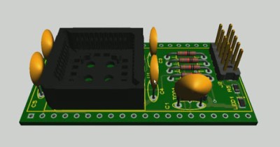
The CPLD: A surface mount part that fits a through-hole socket
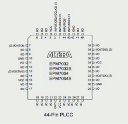
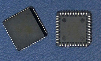 This part known as the EPM7032 and EPM7064, comes in a 44 pin Plastic Leaded Chip Carrier (PLCC) or sometimes called J Lead due to the J shape of the pin leads. This package can be inserted in a through-hole socket or directly soldered to the PCB.
The Oscillator
The on-board oscillator is included so that the CPLD can do things statefully and create fast counters on its own without the need for an external clock. If an external clock is available, the higher speed clock on the module can be used to create a clock event on each rising or falling edge of the external clock and still abide by the guidelines for CPLD/FPGA’s that says that you really should use the internal global clock network and not drive a clock input “asynchronously”. This oscillator is rated for a supply voltage between 1.8 and 5.5 volts.
If you watch the video you will see me discuss my personal preference for how I treat the enable “INH” pin on an oscillator; simply put I tend to leave it floating after I check with the spec sheet that doing so is legal.
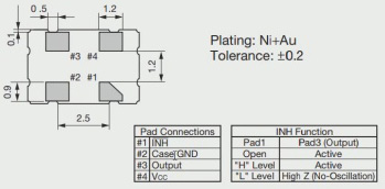
The kind of reasons that flit through my mind when dealing with this sort of function include the fact that I don’t like to tie an input pin directly to a power rail if I can help it. I.E. I prefer to use a series resistor that would limit current during transients, even if it is not supposed to be needed.
Over the years I have seen problems in production (mass quantities) where occasionally something like power cycling will allow a pin tied directly to a power rail to have a higher voltage than the chip itself which is bad. Lastly with a pin tied to a power rail through a resister, whether power or ground, one can change their mind later and use the pin. This is especially true in my experience for unused gates, which as you probably know should never be left floating or unconnected. By using a pull-up you have a point where you can connect a signal and use the gate without having to cut copper traces.
Programming the CPLD
The 10 pin connector and a handful of resistors comprise the programming circuit. If all of the resistors were pull-ups I would use a resistor network but alas, one is to ground.
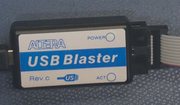 To program a standalone CPLD like this, a dedicated programmer is needed. That’s easy for me to say as I usually have several lying around, but if you don’t have one it’s not too painful to get into the game. An approved “Altera USB Blaster” costs $50 and is available from places like Digikey. I have several clones that I got off of Ebay including one that is a clone that supports Altera, Xilinx and Lattice all in one. There is a project and code available on the Internet for making your own clone and I have it on my list of possible videos to do a project of making a programmer clone. I will also be showing a shield design where the main board, Arduino, PIC, etc., can do the programming
The software needed to compile and program the CPLD is available for free from Altera though the older version 9.1 is needed for this older part. The good news is that it’s my favorite older version that had an intuitive timing analyzer which was removed in later versions.
The PCB
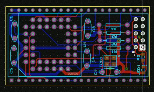 The PCB is a simple two sided design and I tend to do a copper pour for ground and sometimes power as long as the board lends itself to it. Sometimes the pour gets so broken up that it may actually induce issues or just be sloppy in the end result, so again a copper pour is a tool but needs to be managed.
The 3D View
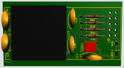
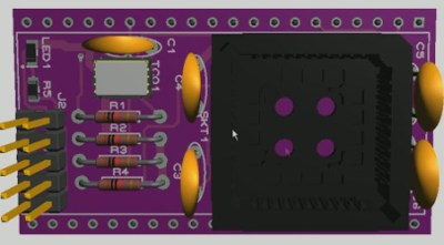
Many if not most CAD packages these days include a 3D view of the end product, though the accuracy of the image it is only as accurate as the 3D models used to represent the parts. Here it can seen where I select 3D model for the 44 pin socket, the programming connector and the oscillator. Here are some of the 3D packages I like to use:
Also many companies have their 3D models for their components. Molex is just one example of a company that does rather well with this.
The Mistakes
The mistakes I made don’t affect the function so much as aesthetics, not counting the main issue which is that it doesn’t fit a single solderless breadboard very well.
Once it occurred to me that I might share the design with anyone I was instantly unhappy with the schematic symbol for the CPLD and for the pinout of the 40 pin connector that is its overall footprint. I had grabbed a 40 pin dual row connector symbol and adapted it to a 1” footprint, however instead of the pins numbering 1,2,3,4… down the side like a DIP package it is numbered 1,3,5,7… like a ribbon cable connector. Consequently it’s a non-intuitive footprint for figuring how to connect to the module and for troubleshooting.
 Likewise the CPLD pinout is a bit confusing, I used a set of utilities that rely on Boundary Scan Description Language (BSDL) to create the symbol. Most of the big vendors have BSDL files available for their mainstream parts and these allow you to create symbols and footprints (semi)automatically. Like any piece of automation it needs to be treated like a tool and may need further massaging for best results. In this case I let it list the pins alphabetically which is almost random when it comes to tracing a pin on the board. Lets just say I was in a hurry that day.
You pay for those shortcuts at some point down the road. When I go to revise this module I will be sure and give it a pin placement that matches the part itself so that knowing where to put your scope probe is as easy as glancing at the schematic symbol.
There are other improvements that are mostly aesthetic or usefule when working with the board. The pin 1 indicator needs to be more prevalent for several packages and I always like an easy ground point for attaching scope grounds or VOM leads. I will probably add this by adding a two pin connector so that power and ground can be applied directly to the board rather than clipping onto the bottom pins.
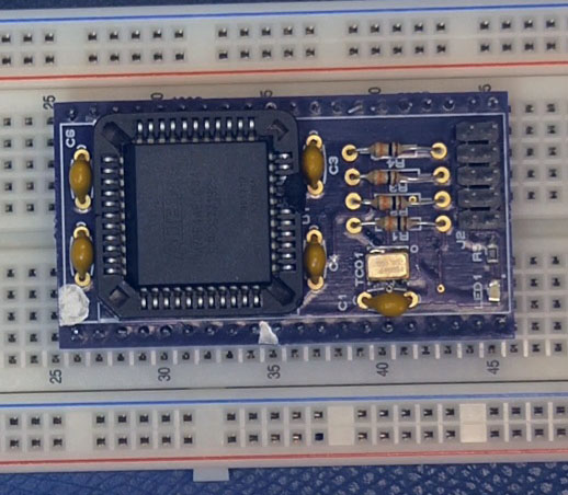
Test Before Revise
 Before I revise the board I want to make sure that it works in spite of the physical and aesthetic issues. After applying power verifying that the oscillator was working correctly I plugged in the programmer and it sensed the CPLD though the 3.3v version was newer than the programming software and showed up as an “unknown” device.
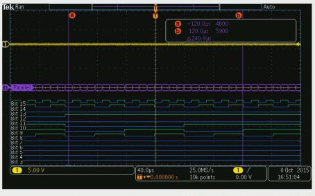
Next I created a counter in Quartus and assigned pin numbers. A quick compile and download and the counter function as seen by the scope verified that the design was viable.
The quick test circuit in Verilog is pretty simple. The code is listed below and you can download A ZIP file containing both schematic and Verilog test circuits as Quartus II Projects (Requires Version 9.1).
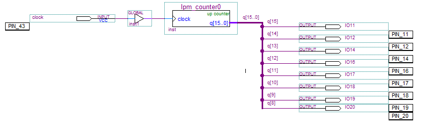
module block1
(
 clock,
 IO11,
 IO12,
 IO14,
 IO16,
 IO17,
 IO18,
 IO19,
 IO20
);
input clock;
output IO11;
output IO12;
output IO14;
output IO16;
output IO17;
output IO18;
output IO19;
output IO20;
reg [15:0] q;
assign IO11 = q[15];
assign IO12 = q[14];
assign IO14 = q[13];
assign IO16 = q[12];
assign IO17 = q[11];
assign IO18 = q[10];
assign IO19 = q[9];
assign IO20 = q[8];
always @ (posedge clock)
 begin
 q <= q + 1;
 end
endmodule
Where to go from here
 As I mentioned I will be doing a second revision of the board paying more attention to the details needed when sharing a design or doing any amount of troubleshooting. Since I need to make the width of the bottom connector .9” or less I may go ahead and make it .6” which is a standard “wide” DIP footprint. Doing so will mean having the underside pins protrude through the CPLD socket footprint. I would not do this in a production situation as it is hand assembly at that point, but then one of the goals was to make a hand solderable kit. The compromise for hand soldering is that the oscillator really needs to be in an SMD surface mount case, the through-hole versions are huge and don’t typically support the voltage range I wanted.
Also I really like surface mount LEDs, I think they look cool.


The definition syntax reminds me of the NAND to Tetris series.
Would it be possible to build up a whole simple computer using these modules? Would need to add ram I suppose.
Lol… yes depending on what kind of computer. However a “real” microcontroller/microcomputer would suffer from the modules being “pin bound” meaning you just can’t get enough terms into and out of the module(s) to do anything too useful.
I did an entire NTSC camera timing and mode controller in the 64 size resulting in no processor needed.
Structural Verilog and the HDL used in the Nand to Tetris book, which by the way is a great peace of literature and definitely worth a read, are more or less the same.
Why through hole parts? Soldering 0805 is easy! It’s about time for every tinkerer to learn that skill.
It doesn’t need to be a rectangle board, maybe place the CPLD 45° rotated, would look funky :-)
Hi Frank!
If I let the socket on the top overlap the pins soldered from the bottom then I could go with “6 centers (emulate a 40 pin chip) or go diagonal, etc. This would be strictly a hand solder assembly at this point to solder the top socket after the bottom side pins.
But it is difficult for a beginner to solder it from the bottom. When I solder pin headers for PCBs for breadboards (these SMD adapter boards which you can get on eBay cheap are useful for prototyping), I insert the pin headers in a breadboard, then place the PCB on it and then I can solder it easily, and it fits the breadboard perfectly. More difficult if you need to solder it from the bottom.
Diagonal mounted it is possible without overlapping, with 4 rows if the CPLD is in the middle (maybe easier to route), or the CPLD can be at one side:
http://i.imgur.com/GVBX0de.png
Can be made small enough so that there are even two rows space on each side on the breadboard.
Thanks for the tip on inserting the headers in to a breadboard prior to soldering. Mine were coming out slightly wonky.
What about a “dongle” type with your breadboard pins in DIP format at one end and the chip socket itself at the other? Chip can hang off the end of the breadboard. Routing would be tight.
ASCII-art on phone attempt
|####### ******************* |. <– Pins 1-20
|##44pl## Osc. port etc |
|####### ………………………. | <– pins 21-40
Open-sourced programmer to go with it would be wonderful.
I will see what that looks like when I go for rev 2.
Yeah I settled for using the “free” version of Altera just as Xilinx and Lattice have “free” versions. I need to close the loop with Al Williams as to just what all the open support does support, which has to include the device family specific attributes. With that said I have done a LOT with the free versions.
If you have a gap in the middle you can do it more narrow, some ascii-art:
———–
########## | | ########## pins
| cpld |
########## | | ########## pins
———-
Ok, the ascii-art didn’t do well, all spaces was optimised away…
Add some spaces between the || and place the cpld there.
Yes, you are showing the CPLD overlapping the pins I believe. That is probably what rev 2 would look like if I follow correctly, When designing for (mass) production I always am allergic to to “hand solder assembly” steps which this is since they overlap (truthfully the soldered pins on the non-component side already were hand solder assy) but then this is just a small kit not a production oriented design. I just have habits that are hard to break at my age. :)
No overlapping. Place the CPLD in the middle then the pins on either side of it.
I think a T shaped board with the CPLD and passives on the wide part of the T, hanging off the edge of the breadboard would work great. Something akin to the Adafruit RasPi T-Cobbler (http://www.adafruit.com/products/2028). This would leave most of the breadboard area free for use.
Too bad it’s discontinued. That will severely limit it’s usage in hobby projects, like with all those XR2206-based and ICL8038-based function generators.
Interesting idea. I love both of those chips. The CPLD isn’t obsolete just yet buy way cheaper at 3.3v.
Hi Bil,
nice tips on pcb design details.
about your “duh”… you don’t really have make a new layout to put this in a breadboard. Just put the wires in the breadboard first and then put the cpld over the wires. Or use 2 breadboards if you can pull the power and gnd strips off of one of those.
About Altium vs Eagle. Did you consider KiCad? It has none of the limits for which you prefer Altium over Eagle and it defaults to generating DRC error for all unconnected pins. You have to tell it if you really want to leave a pin open. (Maybe only for inputd, not for outputs, haven’t checked yet). Another great feature is that’s very easy to learn. Just spending an afternoon wit the excellent getting started manual got me going.
I prefer (the bigger parts of) smd’s above through hole. They are much easier to work with. You don’t have to turn the pcb all the time. (Made some silly mistakes because of mirror image…). and you don’t have to cut the leads of the resistors.
When sharing a design it can be handy to put multiple footprints on a pcb vor a single part. smd resistors an TH. (does complicate layout a bit).
Can I ask which tutorial you used fro KiCAD?
I used “Getting started with KiCad” in pdf format.
The older version I used was 29 pages, and the latest version has 52 pages.
You can find it with other tutorials (including video links) on:
http://kicad-pcb.org/help/tutorials/
I know [Chris Gemmell] of Hackaday and The Amp Hour fame does a series on Kicad http://kicad-pcb.org/help/tutorials/
Kicad might work, let me see what happens for Rev 2, thanks for the suggestion. Unconnected inputs are a good thing for a DRC(ERC) to catch, for connectors and other things leaving them as soft or IO usually avoids disconnected messages on most CADs.
Ran a quick test and threw a connector in an empty sheet, ran annotation and DRC.
It gave me an drc error for each pin.
Marking known unconnected pins is pretty trivial though.
Just out of curiosity, what was the pin type set to on the pins?
It’s set to passive.
I had to search a bit ( Edit Component -> Edit with Library editor.
The library editor opens in a separate window with your component loaded and you can examine or change any part of your component. Changed components can be saved or updated in your schematic.
This makes it very easy to change components. I don’t care much about libraries. If you work with a cpld for example you want to give the pins meaningful names. and it’s much more important that there is a good interface to design your own components.
in KiCad’s ERC a “Not Connected” pin is a separate pin type from a “Passive Pin” and all “Not Connected” pins generate errors.
The way the ERC works kan be easy adjusted to your own preferences in:
Tools -> Electrical Rules Checker -> Options.
This little schematic generates 2 ERC errors. (Green arrows).
Pin 5 is a “Pin not connected” error and the other is:
“Pin connected to some other pins but no pin to drive it”.
KiCad knows that the GND of the 7400 is connected to the connector.
The GND pin of the 7400 has however the pin type “Power Input” and KiCad is not satisfied if it’s just connected to something.
VCC is labeled as being a power net and therefore the VCC pin of the 7400 does not generate an error.
I want to attach a screenshot but it seems it is not possible to upload a picture without creating an account somewhere.
My prototyping setup is 4 solderless breadboards side-by-side. They are glued to a scrap piece of MDF, so they don’t shift relative to each other. I’ve had things that are a similar width (or maybe even a bit wider) that I’ve used by spanning the width of more than one solderless board. It isn’t a good general solution, but it could work for a one-off here or there.
I’ve done that as well. Works a treat once I realized large parts don’t need to be on one board.
I wonder if you could do a vertical board with surface mount right angle pin headers on either side for maximum breadboard space.
I was scrolling through to see if this suggestion popped up–seems like a good solution. Alternatively, maybe mount the CPLD on a separate board that is right-angle soldered to the DIP board?
I have prototyping with CPLD’s lately. Here is what I have found / tried.
PLCC chips are expensive and hard to find. There are many PLCC to DIP adaptors on ebay used for chip programmers. Most of them have the PLCC socket overlapping the DIP. I didn’t bother with PLCC because the chips are always in shorter supply than QFP TQFP and in some cases even DIP lol.
0.8mm (T)QFP is easy as to solder and even so, on home made PCB but this normally limits you to 44 pins.
0.5mm is a fair bit harder but still doable for most people though it would exclude some. However 0.5mm will get you to (T)QFP100. By the time you get to 0.4mm and (T)QFP 144 then you have lost most people using hand soldering.
Oh, and I soldered the TQFP100’s with a $15 soldering iron from the thrift store that had a tip about 3mm round. Just tack some corner pins. BLOB solder one edge – let it cool – clean up the solder with solder wick – let it cool – repeat another three times.
A TQFP44 chip will sit square on a 0.6″ DIP breakout board but it has to be double sided to rout.
There are some 5 Volt tolerant chips that are in better supply than the older 5 Volt chips that I thought were *all* obsolete.
The 5 Volt tolerant Xilinx XC9536XL(36 Macro), XC9572XL (72 Macro) are available in TQFP 44. From memory the XC95144XL was available in PLCC88 and TQFP144. The XC95288XL was in a larger pin count package. Unfortunately Xilinx programmers are more expensive (around $30). These chips are supported by the free Web edition of the IDE.
In the 5 Volt tolerant Altera corner we get a cheaper programmer ($5 – $10), more Macros but unfortunately we have to start with a TQFP100 (0.5mm) chip. There is – the MAX II EPM240 (Equivalent macros 128 – 240) in TQFP100 (0.5mm) and the MAX II EPM570 (Equivalent macros 240-570) in TQFP100 (0.5mm).
72 Macros can get a fair way but it’s the pin count that is limiting. For example you could put a very basic bare bone VGA generator into 72 Macros but you wont have the pins to drive an external RAM unless you use some external bus latches. Well I can’t lol – your mileage may vary.
The Altera chips are a big step up in usability because of the higher pin count and more Macros but at the expense of usability on a bread board. I solder the TQFP100 to a square 0.1″ breakout board that doesn’t have a programming port (a generic adaptor) or buy a minimum breakout from ebay – these have double 0.1″ rows on each side and aren’t really bread board friendly. Perhaps a TQFP100 Altera chip would fit onto a long DIP adaptor with a programming port?
From memory the EPM’s have about 78 – 80 IO. So if you had an on board 3v3 reg, active crystal oscillator and programming port then you only need say 2 power and for the EPM570 that would mean a total of 80 pins or a 4″ (10cm) long DIP. So it’s kind of bread board friendly but it doesn’t like to share the bread board and hence you would need a couple of breadboards.
And one thing about the crystal. I have several breakout boards that have SMD oscillator blocks on them and I want to change them. If they were pin trough then it wouldn’t be hard at all to change them but with SMD – I expect that I am going to break something or lift PCB tracks. I might just put a pair of cutters through the crystal first to save the tracks.
Great overview. Good point on the TCO/oscillator, I am thinking a 3 pin post with jumper to select on-board crystal or external.
I assume most hobbyist don’t really want to do surface mount, I could be wrong on this but then I have a microscope (and I still don’t want to do surface mount hand solder most days).
I think that what a hobbyist can do is more about what is ‘achievable’ with cheap tools and the cost of failure.
For example, a hobbyist might be comfortable to solder a 0.8mm QFP onto a cheep breakout board when the cost of failure is small and they can buy cheap replacements and try again, but they probably wouldn’t take on a large board (at a higher cost) even if it had only one QFP 0.8mm in the middle because the whole project can be ruined.
For one/some of my projects I will have the high pin count SMT chips in breakout boards that plug into the main board so if soldering breaks one, then you can try, try again.
Perhaps two versions. One low pin/macro count and easier to solder and another a little harder with more pins / macros for more advanced projects.
As for the width, I have heaps of breakout boards that are too wide for a middle of a standard breadboard. The easy fix is to get two breadboards and remove the power buses from the closest sides so there is a lager gap in the middle. Personally I have moved away from breadboards (many years ago). Just recently I have re-discovered wire-wrap. I use vero-board as the base and solder sockets and standard header pins and wire wrap from there.
I could see one PCB that could do both a higher density and the through-hole part. As mentioned by others the JLead parts prices are high and going higher so maybe lost cause.
I kind proved I don’t use breadboards when I was completely surprised that I was anywhere near the limit. Did you see my video on wire wrap?
Yep, I bought the same simple hand wrap tool. I have always ha kynar wire because I use it to fix broken via’s / traces on PCB’s.
I have given up on the original wire wrap parts as they’re getting expensive and to hard to find. I use vero-board and solder the sockets to the board and then solder headers beside those. I use ZIF sockets because they’re cheaper than wire-wrap sockets *and* they work fine with the larger pins of breakout boards. The other advantage is that the pinout is not mirrored.
I can get two wraps onto a standard header and that is enough for me. If I need more then I just solder in a length of header along a track on the vero-board to common them.
I can also get 20mm 40×1 headers on ebay but I haven’t needed them yet.
I will try to post a pic.
Here’s a pic – so it did happen!
https://cdn.hackaday.io/images/8326901446090574982.jpg
Nice pic RÖB, the programmer looks familiar also.
Re: removing the SMD oscillator, you could use a hot air rework station, if you have access to one.
Thanks for the great rundown of what’s available out there CPLD-wise!
FYI: $3 Xilinx JTAG dongle using ESP8266. Runs on lua and support Xilinx XVC for remote JTAG. connections in source code.
https://github.com/wzab/esp-wifi-xvc
I haven’t tried it yet.
That kind of project is why I open the question up regarding things like programmers and open source as there is tons of stuff out there that may move the bar that an old fart like me would have a hard time tracking down without y’all.
This article realy came in handy! Early in this week I started to design a similar module with EPM7064S.
Is my first time with CPLDs and has lack of information in Altera’s website about the minimum design (clock, bypass caps, programming) to new ones like me.
I already have an initial layout that I didn’t put on production yet, seems that I’m gonna have a rev.2 before the rev.1 :P
Lol… yeah now that its easy to do PCB layout I get ahead of myself from time to time and usually know the day after I sent the gerbers in that I should have waited a day.
https://www.altera.com/support/support-resources/support-centers/board-design-guidelines.html
There are tons of info, just that they are not at the beginner’s level.
Thanks for the tip!
Bill,
Could you not bridge two breadboards with one power buss in middle? Why only one breadboard?
Err— wait, the pins may not support the weight of the other breadboard, so a breadboard back plane would be in order
What is the spacing when they are snapped together ? (the breadboards)Will it fit? Oh, I smell mission creep….
later Napervillian
Lol… the only reason I own two breadboards is I couldn’t find mine so I ordered a new one. When I went to put it away after it arrived I promptly found the original breadboard.
I should of said design creep.
Just trying to save/ salvage what you have there…
Hey between Rev 1 and Rev 2 is an ideal time to creep.:)
@[Bil Herd]
I just looked at you video. I have a stick (around 20) TI 22V10ACFN’s which I assumed are Texas Instruments 22V10’s but the Texas Instruments chips were (apparently) marked TIBPAL22V10.
Anyway I wanted to use them so I was looking at programmers on ebay. I couldn’t really find any software, apparently there was some free software called CUPL but I didn’t find a download. That and then I remember that these are One Time Programmable anyway.
So I was thinking of buying the one of the two programmers that you tossed over your shoulder. You save me the trouble lol.
PS: Want a stick of TI 22V10ACFN , they’re over 30 years old so they will be 5 Volts, OTP. They’re packages in PLCC28, and four pins are NC so they adapt to DIP24 well.
“It seems that the plugin space available on a solderless breadboard is 1.1”, I had made the footprint 1” wide leaving no room for a row of wires on both sides. Duh.”
@Bil, Maybe I’m missing something here. But surely this is not all that Duh.
Most solderless breadboards can be disassembled into three parts. The power rails on both sides can be pulled off when needed. Simply cut the foam backing tape and yank up one set of power rails. Now, take another breadboard and snap that in instead. You should get more than 1.5 inches to play with. Wish I could show you a picture but can’t figure out how.
Great project, by the way, and thanks for sharing.
Ya it was more the surprise that it wasn’t wider, but then I don’t use them often. I tend to use the little ones in videos and assumed the big ones were bigger in all dimensions.
https://www.brouhaha.com/~eric/retrocomputing/mmi/palasm/
http://www.atmel.com/tools/WINCUPL.aspx
Wow, ok some questions if I may please.
The ‘.for’ files – what language are they? I want to make a GUI (windoze) from them. please don’t tell me Fortran lol.
Linked files to the exe … Wow … you know your downloading *OLD* files when they’re split into 360kB sections to fit in Single Density 5.25 Inch floppy !!!!
Hmm, I might try the Atmel link lol.
Palasm is probably compiled executable for DOS 3 or so. It was one of the common programs as was CUPL and MACH. I shot a whole video on PLDs where I showed how to use the old programs to create state machines and definitions but at the end of the day there was no path towards a workable, programmable part. I still have a copy of AMD MACH still wrapped, I am pretty sure it has 5 1/4″ discs in it.
Atmel’s WINCUPL does run, acts like a Windows version of a DOS program but appears to have been stripped down to support the Atmel families. Mix that with the Ebay programmers that support a random sample but not the whole Atmel family makes it a kinda mute situation.
.for are old FORTRAN source code.
Hi Bil –
Did rev 2 of the board ever happen? A couple of us old farts (and a younger one or two) are building CPLD cards to be used as standins for hard-to-find PDP-8 OMNIBUS cards. One card can be loaded with various personalities to substitute for a range of original cards loaded with discrete components.
See you next Spring at VCF-East.
Lol…. was holding the rev 1 today, its scheduled next to go into the (re)design phase.
Is there a footprint that works better for your app or can you use 1″ centers?
Good timing for me, thanks! The final app will be a custom board, so if your new rev fits a standard breadboard, that will be great to use for dinking around with code and i/o.
I’ve been looking for an excuse to play with a CPLD for a while now, and this project gave me the motivation I needed. Since Bil had done an excellent job in laying out the groundwork, I thought it would be fun to try my hand at designing a little board. I admit I’m a noob at pcb design, so I also saw this as a learning opportunity. I was able to squeeze the size down to where the board can fit within the confines of a 40 pin .6″ dip socket. Anyway, I got the board this weekend and managed to solder it together and test it today, and it works great! For those interested, I uploaded the gerbers, kicad project, bom, and quartus test project to this github repo: https://github.com/jth0mass0n/SimpleCPLD . Maybe someone will find it useful.
Thanks Bil for a great post as always!
I’m interested to see what you did but my system is being re-loaded and I don’t have any PCB-CAD in yet.
Any chance you can put up some pics of the board as image or pdf?
I will go and see if I can find an online renderer for gerber.
Hi RÖB,
i added a couple pics to the github page. For some reason they weren’t showing up earlier. I’m not sure how to post pics in the comments section here. Here’s a link to the picture of the board: https://flic.kr/p/B3MkrC. And then here is the counter running: https://flic.kr/p/B3Mkg7. One way to see what the board itself will look like without having a gerber viewer that I’ve found is to just go to oshpark.com and click on the get started now button, and just upload the Gerbers.zip file from the github page. Hope this help.
I had a look at the Gerbers and BOM.
Somewhere here I have a ATmega664 QFP package that was put on a DIP40 adaptor. The chip is square instead of diagonal and all the DIP pins go through hole normally. So I think you could do this on your board. It would make it much easier to use it to replace older logic chips.
I am assuming that the chip you used is an older one because it’s a full 5 Volt chip. I have been using Altera EPM240 / EPM570 chips (200-500 macros) that are 5 Volt *tolerant* but they are 100 pin and 0.5mm spacing. Xilinx also has XC9536XL (36 marcos) and the XC9572XL (72 marcos) that are 5 Volt tolerant and 44 Pin / 0.8mm like the chip you used.
Looks good though. I also have breakout boards that are missing the middle pins.
The old chips (most) had GND and 5V positioned in the same way. With the chip upright (pin one at top) GND was the bottom left pin and Vcc was the top right pin.
Some of the early SMD QFP chips had pin 1 in the center of an edge instead of one corner.
That QFP to DIP40 adapter sounds perfect for this type of board. All in all I’m happy with the way this board came out, I do wish I could have thought of a way to keep those middle pins in the design though. I’m sure I could fit them in if I pushed the rows apart another .1 inches.
I chose the 5v chip just because I’m interfacing with a lot of old chips from the 80s that had that same voltage requirement. But I believe the 3.3v tqfp package would also work with this board. You’d just have to change the 5v labels to 3.3v on the silkscreen. Thanks so much for the heads up on the XC9572XL! That looks like quite a nice little package. It gives me an idea for another board now.
I also have some boards where the center pins aren’t drilled through the PCB. And you use a combination of SMD / pin through connectors. It’s hard to explain so I will put a pic up.
I wanted to add some info about the work I’m doing to impersonate old DEC FlipChips with a CPLD in the same form factor as the original board. The card would be loaded with the appropriate code for the function needed. I’d like to be able to put up some images but I don’t see a way to do that, though obviously you guys know the trick. What’s the secret?
@[Jack Rubin], There isn’t really a secret to images. Just post the link. I take the ‘s’ out of https because that sometimes helps. If your a regular user here then your post will come straight up. If you’re not a regular then your post may need to be moderated to get rid of spam.
http://cdn.hackaday.io/images/7805741449733809087.jpg
RÖB: I like the look of those boards! I saw something like that on ebay, but I hadn’t a clue how they connected to the pins in the middle. Thanks for the pics!
Jack: I haven’t tried posting pics yet, but I think you can just use an html img tag possibly to do the trick. Or just paste in the url to the images and we can click the link.
Excellent follow up guys. Also I have just re-laid out the PCB for .6″ Centers and jumper selectable clock. I did eliminate the power indicating LED due to space. I am trying out a new (for me) Chinese PCB manufacturer where 25 boards was $23USD so I will see how well that works.
dirtypcbs.com/ ?
Hello,
This is great.
Do you have the actual Proteus project files you made for this available for download?
Thanks
Hello. Can you describe how you got the Generic USB blaster to work with Quartus 9.1 SP2 on Windows 7? I cannot get the drivers to work. Keep getting error code 10.
Quartus, unlike many software packages, can have multiple versions present at the same time. My memory is I got one system to work by loading a newer version of Quartus (like 11 thru 14) and then finding the directory for the USB blaster and installed that driver.
Thanks I got it working by using the drivers from a later version.
only epm7032s have jtag
Hi,
Do you, by any chance, also know how to extract the program from a MAX3000A given its Security bit was enabled?
Hello, I look for reading a microchip NEC DP784046CG(A1) from ECU of Honda Silverwing Motorbike.Someone can help me?
Anyone here have a copy of Quartus II 9.0? You can no longer download it from Intel, They have some Max 7000 support in 13.0 (oldest available version), but it does not list my chip EPM7064SLC44-10
Hello.
I saw your project on cplds. I downloaded your design to change the presence of the TCO; I will add it externally.
I wanted to know: the series of 0.1 uF capacitors must necessarily be polarized electrolytic, or can I replace them with plastic capacitors?
Thank you for the project and for your availability
Hello,
as I saw nobody mentioned that earlier but the PCB gerber files contains a 4 layer design instead of a “simple two sided design”. I checked with JLC’s and OSHPark’s gerber view and in fact, there are side pins that are not connected either on top or or on bottom copper layer.
Note: rev2 is 2 layer design
EPM7032S – JTAG UNLOCK – first time without clear IDCODE!!
It is now possible to unlock the MAX 7000 (EPM7032S) and reprogram it with Quartus and USB Blaster!
Using my Parallel Programmer – Arduino Mega, I was able for the first time to erase an EPM7032S (JTAG UNLOCK) without erasing the IDCODE.
https://www.eevblog.com/forum/fpga/programming-(non-jtag)-max7000-devices/msg6159005/#msg6159005