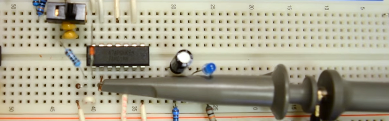
Solderless breadboards are extremely handy. You always hear, of course, that you need to be careful with them at high frequencies and that they can add unwanted capacitance and crosstalk to a circuit. That stands to reason since you have relatively long pieces of metal spaced close together — the very definition of a capacitor.
[Ryan Jensen] did more than just listen to that advice. He built a circuit and used a scope to investigate just how much coupling he could expect with a simple digital circuit. Better still, he also made a video of it (see below). The test setup shows a single gate of a hex Schmitt trigger inverter with a sine wave input. The output transitions ring and also couple back into the input.
Of course, the circuit is simple. Some additional decoupling might have helped some. Still, [Ryan’s] circuit isn’t atypical of something you’d see on a breadboard, so his points are still valid. Another thing that can help is mounting the breadboard on a solid ground plane.
Towards the end of the video, [Ryan] guts a breadboard to show what’s inside. We’ve seen people do surgery on the breadboard internals before, but if you haven’t seen one eviscerated before, you might find it interesting.


I like the video, but he should’ve tried the same circuit/testing without the metallic backplane he peeled off near the end of the video.
It may have been making the problem worse.
Do you mean the bit he starts peeling around 3:30? Don’t think you can pull off just that. It looks like it’s metal > adhesive > breadboard contacts, so he couldn’t get just the metal plate off.
Now I know why my breadboard radios never worked when I transferred them to a PCB.
He didn’t show how he drove the input of the Schitt either. It might be “flappin’ in the breeze” as EEV-Dave would have said…. If if was driven stiffly enough the 4pF capacitance between the breadboard rows might have been negligible.
What kind of trigger is flappin’ in the breeze? Freudian slip?
I think your on the money there.
But good on hm for taking the time to video the effect. It was a nicely presented video
I can remember plenty of times Dave has used “flappin’ in the breeze” for caps that have no silastic but not for describing a floating input. I could well be wrong though.
I wonder what the parasitic of that big honkin grey probe was.
But since it is used in both cases, it can be considered negligible.
Not negligible! Typical oscilloscope probes are 12p input, and cheap ones even more.
The picture show that the external ground wire is being used with the scope probe which is not recommended if you are trying to do any accurate noise measurement. The ground wire has a huge loop area, and that can alter the signal enough to affect your reading.
https://e2e.ti.com/resized-image.ashx/__size/550×0/__key/communityserver-wikis-components-files/00-00-00-02-43/4544.noise_5F00_with_5F00_probe_5F00_GND.png
I whish our high end scopes had a ground pin like in the second picture. They have this ridiculous mosqito leg kind if thing that makes a loop anyway. I roll my own with a piece of spring that I bend a leg on. Works very well.
i thought most oscilloscope probes do come with a hook like that…just that people ignore the tiny wire in the bag or simply lose it.
Yeah and that’s ok but I want high end probes to go with the high end scopes. Or maybe I just wanted to brag about my spring trick… Sorry, I’m very tired right now.
https://e2e.ti.com/resized-image/__size/550×0/__key/communityserver-wikis-components-files/00-00-00-02-43/4544.noise_5F00_with_5F00_probe_5F00_GND.png
i didn’t understand this working
“That stands to reason since you have relatively long pieces of metal spaced close together — the very definition of a capacitor.”
Wait, what? A normal board, with a ground plane, has big giant pieces of metal spaced close together, too. The parasitic capacitance is tiny for a breadboard. Heck, it’s smaller than a normal PCB.
It’s the *inductance* that’s huge on a breadboard, because the return current is forced to be far away, because, well, it’s a breadboard, and most people don’t think about routing return currents close to their signal. And inductance is proportional to the loop area, which can be very big.
So you’re saying that two reasonably short traces on a PCB have comparable capacitance between _each other_ that two adjacent breadboard strips…?
The metal contact have parasitic capacitance. Normally that is only an issue for analog circuits (oscillators, high impedance circuits).
Now the much bigger issue for digital circuits is the inductance. See my post below. The jumper wires, the contacts etc are inductors and magnetic coupling can cause crosstalk if you don’t have good return paths for signals.
No, I’m saying the parasitic shunt capacitance to a supply is smaller (if, for instance, you’re making a filter or something). The parasitic capacitance between two traces is very, very often negligible, because the mutual inductance is higher.
Imagine if you’ve got a breadboard with trace A and trace B in adjacent strips. Unless their adjacent strips are grounded, they’re almost certainly sharing a good portion of their loop area. And the loop area will be *big*, so the inductance will be big, and the mutual inductance will also be big.
Parasitic capacitance is just never that big. Roughly estimating, let’s say 0.1″ spacing, 0.2″ strip width, air dielectric, it’s going to be around 0.0174 pF/mm – so for a strip that’s, say, 10.16 mm long (5 holes) that’d be 0.18 pF. Parasitic *inductance* is so much more of a bastard – it’s typically in the nH range even for a PCB. Which isn’t really surprising, since the vacuum permittivity is so much smaller (~8.8 pF/m) than the permeability.(~1.2 uH/m).
+1
If there is no close by power or ground return path for the current, then the closest signals will be used leading to crosstalk. These types of crosstalk are magnetic in nature as we are dealing with AC currents and the parallel metals strips of contacts can act like transformers.
These big copper areas are usually power and ground and act as a free shunt capacitance. Having capacitance between an output and high impedance input is bad. If the board designer knows what s/he is doing the right choices are made of what goes together and what is separated. Hobbyists breadboarding does not always have this insight and think it is enough with electrical connection between the nodes. This is a very good topic to make people aware that some thought need made even if you just doing a quick prototype.
Capacative coupling between traces is typically tiny. There’s just not enough area at close separation, even on a breadboard (and 100 mil separation isn’t exactly close). Inductive coupling is easier: you just need shared loop area, and on a breadboard, unless you provide a ground path for each signal, that’s guaranteed.
I was referring to plane areas not adjacent traces. I should have written “Having coupling between….”
And your scope probes are compensated to minimise capacitive loading on the device under test, right?
This is why nearly everyone I knew that started to get serious in analog electronics in school quickly outgrew breadboards for perf and copperclad. Add the parasitics and leakage to the poor reliability…and, meh.
I built many feasibility and pre-production prototypes while working at Xerox and NEVER used a breadboard.
It was all “point to point” soldering or wire-wrap technology. Breadboards like this were seen as just an invitation for extra problems and not an indicator of actual production PCB performance.
On the other hand one could argue (albeit with tongue-in-cheek) that if you can get your design work on a solderless breadboard you’d have enough safety margins for bad routing, bad/substandard components and tolerances of parts when done properly on a pcb in production… :-)
You haven’t taken Murphy’s Law into account. The excess capacitance and inductance will be sufficient to slug the bandwidth and prevent oscillations. Maxim: “oscillators don’t, amplifiers oscillate”.
Yeah. As an electrical engineer, I just never use ’em. I trust datasheets, and know how to read ’em…so if it doesn’t work when I put it together, there’s some real headscratching to do…and I don’t want the breadboard to get in the way. I can’t believe how people keep breadboards around for permanent projects now.
Bigger problem with fast logic on breadboards is parasitic inductance due to large loops. Remember V=Ldi/dt where di is the transient switching current, and google for “ground bounce”.
or just to little ground connection, had it with a video synth i was building..
And speaking of breadboard parasitics…..no mention of the contact resistance. Use your breadboard for too long and it starts to increase significantly.
I was never a fan of breadboards. Good for recycling components after, but so many things did not work on a breadboard because of parasitics.
I used that breadboard capacitance intentionally as part of a circuit, once upon a time. I remember it being equivalent to a few pF.
yeah, my favorite is skipping the 10ish pico caps for oscillators.
Yup, every breadboard is nothing but a big array of “gimmick capacitors” and a big power loop that’s guaranteed to “bounce”.
Non existent power supply decoupling is very likely the biggest culprit here. He is basically supplying current to logic gates through long wires (breadboard traces) which act as inductors and resonate (hence the ringing).
This is a common error, particularly among newbies, most think they don’t need to filter DC because they’re using ultra stable power supplies or batteries, which is wrong. Filtering and decoupling are different beasts.
Decoupling is needed to lower the impedance of the supply source and is what stops any load current to propagate to supply lines. Lack of decoupling can produce ringing or even self oscillation in some ciruits. Typical example is the small audio amp that works fine from a wall wart but motorboats like crazy if operated on batteries. The reason is the high internal resistance of batteries which allows any current fed into the load to propagate back to the amplifier chip, hence to its inputs. Putting an electrolytic cap in parallel with power supply lines as close as possible to the amplifier chip solves the problem instantly. In this case there should be an electrolytic on the breadboard supply line and (most important) a smaller value ceramic connected to the IC supply pins like he correctly did in the final soldered prototype.
In general, if you’ve got a large-value electrolytic and a smaller ceramic cap in parallel, the “closeness” of the electrolytic doesn’t matter. It’s only dominant at frequencies where the inductive reactance due to the distance from the chip is small. It’s the ceramic’s distance that matters much more.
Bingo! This was the first thing I noticed on the video. Fix the decoupling first, then repeat the exercise.
So here’s a semi-newbie question – why doesn’t every modern chip include on-die de-coupling caps? They are critical to most digital environments, and all analog environments above (say) AF. So why not guaranty the best possible operation of your chips by building in the de-coupling as close as physically possible to the internals?
Die capacitance requires *huge* space to get to uF-level caps. Remember, that simple 0.1 uF cap is actually lots and lots of metal plates, stacked really close together, with a dielectric between them. A chip’s *die* is just a single wafer.
You could have *in-package* capacitance, and plenty of high-end chips do that. For lower end chips it’s not practical, because it adds a lot of non-standard stuff to the packaging step. Plus, the package doesn’t have an internal “ground plane”, so you would have to somehow bond-wire the power/ground connections – and that’s actually a lot of inductance.
Some chips are packaged more like a sub-PCB assembly (often times a flip-chip die mounted directly on a substrate), and so in those cases it’s completely reasonable to add capacitors on top as well (plus a ground plane, often). You see that in processors, FPGAs, etc.
To put the magnitude of ground bounce in perspective… Blindly applying the rule-of-thumb at http://www.edn.com/electronics-blogs/all-aboard-/4429476/How-to-estimate-ground-bounce-in-a-connector–Rule-of-Thumb–8 indicates a 1ns+5V+100mm/4″ wire => 10V bounce! Clearly that won’t happen, but it indicates that this circuit is highly likely to encounter such problems.
Also consider where outputs are driving transmission lines with an impedance around 50-120ohms. Even with medium speed logic, you need to think in terms of transmission lines when the interconnect is more than an couple of inches long.