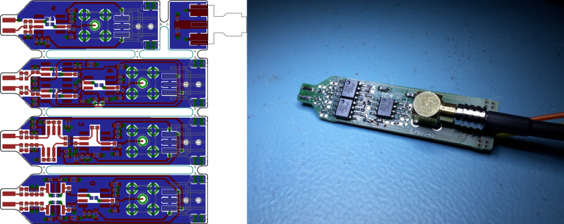
Fancy measurement gear is often expensive to buy, but some bits of kit are entirely DIY’able if you’re willing to put a little work into the project. [Christer Weinigel] needed to get some measurements of a differential clock signal that was ticking away around 500 MHz. El-cheapo probes aren’t going to cut it here. They won’t have the bandwidth and most off-the-rack probes are single-ended, that is they’re referenced to ground. [Christer] needed the difference between two balanced signals, neither of which is grounded. In short, [Christer] needed a high-frequency active differential oscilloscope probe, and they’re not cheap. So he built one himself.
 The circuit in the probe is really just an instrumentation amplifier design with a modified input stage and a 50 ohm output impedance. (See this article on in-amps if you need to brush up.) With higher frequencies like this, it’s going to be demanding on the op-amp, so [Christer] spent some time simulating the circuit to make sure it would work with his chosen part. Then he made up a bunch of PCB designs and had them made. Actual results matched fairly well with the simulation.
With some minor tweaking on the input damping resistors, he got a tool that’s dead flat up to 300 MHz, and totally usable up to 850 MHz. If you tried to buy one of these, it’d set you back the cost of a few hundred lattes, but this one can be made for the price of one or two if you get the PCBs done cheaply. Of course, the design files are available for your own use. Kudos [Christer].
Edit: By total coincidence, Bil Herd just posted a video intro to differential signals. Go check it out.
And thanks to [nebk] for the tip!


The “nomal” ones cost a fortune because they are not referenced to earth. Their input is potential-free. This one has no galvanic isolation. But nevertheless it’s a great thing!
Which differential probes are NOT referenced to ground?
That circuit looks significantly simpler than I’d’ve imagined. Excellent! Maybe even doable by an all-thumbs-at-analog dude like me.
A side-note… Recently learned the easiest way to take a differential measurement with a regular-ol’ probe… run the circuit off a battery, plug your probe and its ground anywhere you like! (not sure how this’d work in all cases, e.g. 100+MHz speeds with weak signal sources… Do we have to consider things like the capacitance between the entire circuit and the room’s plumbing at that point?)
Anyways, thanks to https://hackaday.io/project/9068-measuring-dvd-rw-laser/discussion-44512 for indirectly teaching me that trick 20+ years into my endeavors.
And thanks, this project, for showing me an active-probe may actually be within my means.
Erm, no edit… This is a better link: https://hackaday.io/project/9068/log/29899-weird-noisy-intensity-vs-current-curve The picture is what did it for me.
There are transformers with 1:1 ratio for insulating DUTs or instruments from earth-referenced mains. Useful especially if one is designing or fixing switching power supplies…
Most 1:1 (Isolation) transformers pass the Earth GND pin through the isolation barrier. Which can also break neutral isolation, as (in US electrical code) the Neut is tied to Earth GND at the panel.
The less-safe option is to float your ‘scope or device under test using a 2-prong cable coming out of the isolation transformer. Slightly more safe is to float your device under test (although it may cause different behaviors if you do that, and still allows an Earth GND path to enter your circuit).
Much better option is differential probe like above. Best option is fully-isolated diff probe.
Bestest option is fully-isolated diff probe someone else bought you :D
maybe a solution can be found where (as in some analog input stages) AC and low frequency / DC content are transfered separately across the barrier (DC transfer via a closed-loop solution, AC magnetically coupled)?
The Tektronix THS700 does almost exactly what you describe for its isolated scope inputs. See the second link here for schematics:
http://www.eevblog.com/forum/testgear/tektronix-ths700-tekscope-component-level-information-package-and-schematic/
DC (CH1SLO) is passed over the isolation barrier with an optocoupler. The optocoupler contains two matched photo diodes, the output from one is fed back to the input stage, the output from the other one is fed to the sampling ASIC.
AC (CH1FSTP/CH1FSTN) is passed over the isolation barrier with a transformer.
journeymanwizard, I think you misunderstand. Due to the way the inputs are coupled to the input OP-AMPs on this probe the signals being measured have to be within about +/-3V from ground on the probe. Thus the probe and the scope has to be grounded relative to the device being measured. If you try to measure a device that has a ground which is at 50V relative to the probe and scope ground you will most probably fry the OP-AMPs on the probe.
“differential” on this probe only means that it amplifies the difference between the two inputs as long as the inputs are within the common mode range of the OP-AMPs. It can be used to measure a differential signal such as a LVDS clock, but it can also be used to measure a single ended signal relative to a nearby ground pad. Minimizing the loop area between the signal and nearby ground pad minimizes the noise picked up through that loop. Measuring the difference between the single ended signal and the nearby ground pad lets the instrumentation amplifier cancel out some of the noise picked up through the longer ground path from the probe ground to the device ground.
If you want galvanic isolation and want to measure DC you have to do something similar to what the Tek THS700 scope I linked to is doing. That’s a totally different thing.
cant you just run it off a bench dc supply with out the earth tie on the neg? pretty sure dave on the eev blog mentioned that as a valid way to go in a video titled something like “how not to blow up your scope”
if its a dc device cant you just run it off a bench dc supply without the earth tie on the neg? pretty sure dave on the eev blog mentioned that as a valid way to go in a video titled something like “how not to blow up your scope”
This probe is limited by the supply voltage to the OP-AMP anyway, so it won’t work with anything much beyond +/-3V or so. It’s really only meant for probing decently fast low voltage signals, for example a differential LVDS clock or a single ended CMOS clock. It’s also meant for DC signals, if you connect one input pin to ground and another to a 2.5V rail it’s going to show 250mV on the scope. So a transformer on it’s own won’t work.
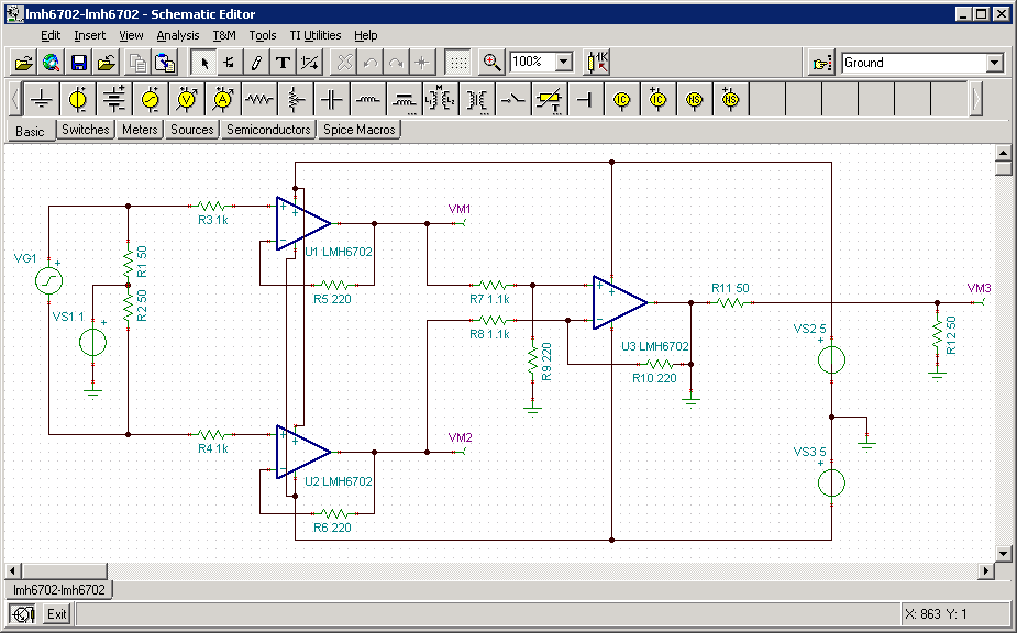
Maybe I don’t understand that schematic:
1. Why is the output of U3 grounded? That looks like there will be no output from this circuit.
2. Why does R12 exist? 50 ohm impedance matching is already provided by R11. Adding R12 makes the output impedance (as seen by the line) 25 ohms, doesn’t it?.
3. If U1 and U2 are acting as voltage followers, what is the function of R5 and R6? Why are they not zero?
Can’t answer Q1 and Q2 (and I’m curious too), but Q3: the input capacitance of the LMH6702 is 1.6 pF, and together with the 220 ohm resistor this results in a low pass filter at 452 MHz. The voltage follower would then see a damped voltage above that frequency, and so boost higher frequencies in order to compensate.
I think that’s the reasoning.
The LMH6702 is a current feedback amplifier. You need the 220 ohm in order to be stable.
I dug a bit deeper about that stability that you mentioned.
In this document: http://www.ti.com/lit/ml/sloa080/sloa080.pdf , paragraph 8.8, it says:
“When designer lets the circuit board introduce stray capacitance on the inverting input
node to ground, it causes the impedance ZG to become reactive. ”
(In this case, the input capacitance of the opamp is similar to stray capacitance on the inverting input.)
The document then shows a nice picture of the influence that even a stray capacitance on the inverting input of 2 pF can cause a 3 dB peak (ringing), and it also increases the bandwidth of the entire filter by 18 MHz.
This was a learning experience.
Anyway, the datasheet of the LMH6702 indicates that a feedback resistor of 237 ohm resistor is optimal, whereas lower values increase ringing. The author did choose a lower value. I assume 220 ohm was chosen because it was more convenient somehow (probably on stock). The writeup goes into some detail about how he was varying R1 and R4 to compensate ringing. Basically by decreasing the low pass corner frequency of the non-inverting input.
He was successful, but perhaps increasing the feedback resistor would be more successful.
So I wonder how much the performance would improve.
Any comments? I suppose you can’t really say something definitive unless you try…
Yes, the resistor value used is just because 220Ohm is a common value for resistors (E12 series) and 237Ohm is not. In many ways I think I lucked out on the component selection.
The 220Ohm feedback resistors are slightly smaller than the recommended value and together with stray capacitance will cause peaking which will decrease the stability and increase the bandwidth of the OP-AMPs.
The 150Ohm input resistor together with the input capacitance of the OP-AMPs and stray capacitance from the PCB forms a low pass filter. If I assume that the total capacitance is about 1pF this filter would have a bandwidth of about 1GHz.
And it just happens that the low pass filter at the input compensates rather well for the peaking in the OP-AMPs giving a fairly straight frequency response for the whole probe. I have since tried a few other OP-AMPs and they did not work as well the LMH6702, they either have too much bandwith which gives much peaking and makes the probe unstable or have too low bandwith which gives a much lower total bandwidth and I haven’t been able to compensate for that with a different input resistor.
I really should write another post on why I think the probe works as well as it does. And then wait for somebody who really knows analog eletronics to come and tell me why I’m wrong. :-)
Answering to Christer ^^
Well I’m impressed anyhow that it works as well as it does.
What I would really find useful is if the probe would have at least a 500K input impedance. Those probes are quite expensive. Then it could measure circuits without loading it too much.
I suppose it also opens up quite a big can of worms… I once tried to create a source follower circuit with FETs to work on 400 MHz at high impedance and low capacitance, but sadly failed.
mime, my probe does have a >500kOhm input impedance, at least at DC. The non-inverting input of the LMH6702 is specified to have a 1.4MOhm resistance. At higher frequencies it’s the 150Ohm input resistor together with the 1.6pF non-inverting input capacitance (and any parasitics) that will dominate.
*tries to remember how to calculate reactance* *fails* *googles* X=1/(2*PI*f*C)
Assuming that the 1.6pF at the input is a perfect capacitor, at 400 MHz the reactance for the input ought to be 1/(2*PI* 400E6*1.6E-12)=250Ohms.
But even the $5k probes from Tektronix aren’t much better than this. They have an input resistance of 100kOhms or so at DC and 0.3pF of capacitance which would mean about 1.3kOhm reactance at 400MHz. Even a SMA connector has a capacitance on the order of a dozen fF or 33kOhms of reactance at 400MHz.
^^ pretty good then. So.. what now then, do you have any plans for version 1.1?
I’ve read things in the past about using “active shielding” or something like that; the output of the opamp is circling the negative input pin of the opamp to reduce effects of capacitance to ground. That would effectively add a parrallel capacitance to the feedback resistor, something that was also mentioned in the document I pointed at earlier. That could increase/improve the bandwith.
Dunno. :-) Adding a parallel capacitor to the input resistor sounds like a bad idea, it would reduce the input impedance and increase loading. I think.
But well… It would be interesting to build one more probe with exactly the same components just to see if how much difference individual parts make. I might have been lucky and gotten two LMH6702s with lower input capacitance than specified. Since I don’t have any control over stray capacitance just mounting the LMH6702s slightly differently might change it. I might also have been lucky in getting two LMH6702s with the same gain and DC offsets, if I get two that have individual differences that could introduce DC offsets or gain errors in the output. I’d also like to try a few more kinds of OP-AMPs just to see if I can find one that works even better than the LMH6702.
I ought to try building variant C with a dual OP-AMP as the input stage. If individual differences affect the performance, using two OP-AMPs in the same package ought to minimize individual differences. Variant D with a fully differential OP-AMP as the input stage might be even better. Another variant would be to use a resistive divider at the input to attenuate the signal instead of doing the attenuation at the second stage OP-AMP. Putting a 5:1 divider at the input would allow the probe to measure about 3*5=15V instead of just 3V. But since there wouldn’t be any attuenuation after the input stage, any difference between the DC offsets of the input OP-AMPs would be magnified compared to now.
Other than that I’m thinking about building an USB powered DC-DC converter to make the probe easier to use. Right now I need to power the probe from a power supply which can deliver +/-5V which is a bit cumbersome. It would probably also be a good idea to add some LDOs on the probe itself to minimize noise on the +/-5V powering the OP-AMPs. It might not make any difference though, the PSRR of the LMH6702 is 52dB typical and the CMRR is 48dB typical. Any noise coupled through the ground wires, which changes the common mode, will probably make a bigger difference than noise on the power supply.
Another thing I’m thinking about would be to use a SATA or E-SATA cable to connect to the probe instead of using a MCX or SMA connector and a separate connector for the power supply. A SATA cable consists of two differential pairs with individual shielding, I could use one pair for a differential signal from the input stage and another pair for the +/-5V power supply. I’ve built a small PCB to test SATA cables and from my first quick test it seems that the bandwith of a SATA cable is a bit too low for this to be doable, but it would have been very neat if it had worked. I’m planning to do a blog post about that but I I’d like to check the frequency response of the SATA thingy on a network analyzer before I blog about it.
I have a bunch of other projects I’m working on. I just built a GPIB adapter to be able to talk to my Tek 11801B scope a bit faster than over a serial port. I want to finish the firmware for that one and blog about it too.
Too many things I’d like to do, too little time.
No, you misunderstood; not adding capacitance to the input resistor, but effectively to the feedback resistor. A guard ring would reduce the input capacitance (effects).
A sata cable has a 100 ohm impedance though [1], instead of the 50 ohms your scope expects. That should introduce reflections at the frequencies that you’re using.
Another idea may be to find a dedicated opamp type just to properly drive the cable.
To minimise the input capacitance you could find a smaller opamp package in the preamp stage?
Your idea of reducing the input voltage divider by a datasheet would increase the maximum bandwidth of your opamp (check your datasheet); reducing the input voltage to 0.5 Vpp would increase the bandwidth to 1700 MHz.
Anyway, I fully understand the “too much to do, too little time” ;)
[1] http://www.sersc.org/journals/IJCA/vol7_no8/15.pdf
Regarding the active shield. I see. As I wrote in the blog posts, I’m really a software guy, I’m slowly learning more about analog stuff. :-)
For the SATA cable, in that case I had planned to feed the differential output from the input stage through the differential pair and put the differencing amplifier at the other end. Depending on the frequency response of the SATA cable it might be possible to compensate for the drop-off in gain, but I’m not sure.
I did consider using the LMH6702 in a SOT23-5 package, but decided to go with the more common SO-8 to have a wider selection of OP-AMPs to choose from. If I’m going to do a second version of the probe I’ll probably use the SOT23 since as you say it does have slightly less parasitics.
Yes, the small signal response of the LMH6702 is supposed to be faster than the large signal response. On the other hand, I’ve done most of my measurements on a 1V PtP signal so I think I am down to the small signal response already. But yes, the resistive divider would make sure that most signals I’d want to measure are small signals.
I’ll see if I ever get around to it.
For point 3, the LMH6702 has a current feedback topology. You need R5/R6 for stability.
1. Oops. The ground at the output from U3 is a bug, it shouldn’t be there. I was trying to model the effect of parasitic capacitance by adding capacitors to ground in a lot of places and when I cleaned up the schematics I messed up and shorted the output to ground instead of removing the ground as I should have.
2. R12 simulates the 50Ohm input impedance of the scope.
3. See espitall’s comment below.
i got on a kickstarter for a cheap 500mhz differential probe that was a total piece of crap … if this works any better i might make one up
i am curious to see the actual input impedance graph … thats what really boned me on the kickstarter one
Also to add, apparently input is 50 ohm referenced from each input to to ground (R1,R2) also, that is just too low (high probe loading) in most cases…
No, R1/R2 are not part of the probe, they are meant to represent a differential termination that I’m doing measurements on.
Wasnt Bunnie or Xobs playing with one during novena development? remember him hacking diff probe from some fet opamp and being surprised how we;; it worked.
I don’t understand why you have decided to have 5:1 attenuation in the 2nd (diff-amp) stage? There is no point of doing that. If you wish to attenuate signal to make a HV probe, you have to attenuate it on the very beginning of the signal path. As all 3 op-amps are identical you won’t gain a bandwidth as the first stage with unity gain will be limiting it.
If “HV” means high voltage, my goal was _not_ to make it a high voltage probe, my goal was to make a low voltage probe with as much bandwidth as possible while keeping the input impedance as high as possible. The first two OP-amps are used as high impedance buffers. Adding a voltage divider at the input would lower the impedance which defeats the purpose of the buffers.
I did create a PCB variant which uses a fully differential amplifier which was supposed to have a voltage divider at the input, but I never got around to actually assembling it.