One of [CNLohr]’s bigger claims to fame is his process for making glass PCBs. They’re pretty much identical to regular, fiberglass-based PCBs, but [CNLohr] is building circuits on microscope slides. We’ve seen him build a glass PCB LED clock and a Linux Minecraft Ethernet thing, but until now, [CNLohr]’s process of building these glass PCBs hasn’t been covered in the depth required to duplicate these projects.
This last weekend, [CNLohr] put together a series of videos on how he turns tiny pieces of glass into functional circuits.
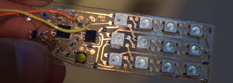
At the highest level of understanding, [CNLohr]’s glass PCBs really aren’t any different from traditional homebrew PCBs made on copper clad board. There’s a substrate, and a film of copper that is etched away to produce traces and circuits. The devil is in the details, and there are a lot of details for this build. Let’s dig deeper.
To bond the copper to the glass slide, [CNLohr] first preps the materials by degreasing with acetone, and rubbing the copper with steel wool. The glue is Loctite 3301, a low-viscosity light-curing glue that can be squeegeed between the copper and glass, then exposed with a grow lamp.
That’s enough to get the copper on the glass, but several steps away from a circuit board. To etch the copper, [CNLohr] is using Riston film photoresist. This is applied by floating it onto the copper with a few drops of water and putting it through a laminator. The laser printer photomask is floated onto the Riston with some 3-in-one oil, the photoetch exposed, and then removed.
The next few steps – washing off the uncured photoetch, etching the copper, and washing off the cured photoetch – are the parts of this process that have given [CNLohr] the hardest time. He needs to use chemicals that don’t interact with the bond between the glass and copper. He’s found sodium carbonate works well for removing uncured photomask, ferric chloride for etching copper (although we’ve had good experience with cupric chloride and peroxide), and potassium hydroxide to remove the cured photomask. With the cured photomask removed, [CNLohr] has a perfect glass circuit board.
Of course, building a glass PCB is useless without soldering components to it. For that, [CNLohr] is using bismuth solder paste for low-temp hot plate soldering. If you’re only doing single-sided SMD work, this is a great way to produce beautiful circuit boards made of glass, but now we’re wondering if a small enough diamond drill bit would allow for double-sided construction.


I want to know he solders the big pads without cracking the glass. Glass like that hates thermal differences.
To lower the temp. difference, a little bit of Pre-heat may solve this issue.
As it turns out, this is really only critical on annealed glass I found out… I have yet to crack a microscope slide (they’re on tempered glass) with the heat… but as a precaution, I do turn the heat down and try to use the low-temp solder paste.
To lower the temp. differences, a little bit of Pre-heat may solve this issue.
“low-temp hot plate soldering”
I’m guessing keeping it all evenly heated is what keeps it from dying.
Bismuth solder paste on a hotplate.
I’m curious as to whether this would work well on a vacuum tube or a Nixie.
Would look great to have digital chips stuck to ‘ancient’ technology.
One could use glue/epoxy and thin wire, but the slides came out looking so good!
I’m not very good at soldering anything so it would be pointless for me to attempt this anytime soon.
Cool to see the whole project described, now all we need is for someone to build a roomscale computer with these, would be a piece of art.
On the widows. Or a glass table. :)
Houses made of glass are a thing.
http://www.santambrogiomilano.com/#!the-glass-house/c81d1
http://static.wixstatic.com/media/0e9ce5_d59f7fc524a44a7a8daf53e887806042~mv2.jpg_srz_1473_737_85_22_0.50_1.20_0.00_jpg_srz
seems like an awful lot of fuss why not just do vacuum deposition
What sort of gear do you need for that, and what size budget would it take to set up a workflow? And why would you want to make glass PCBs in the first place? You can just ink jet gold chloride onto a matt ceramic tile and fire it high enough to get pure gold tracks it if you want something fancier.
Gold will not adhere to glass or ceramic tile very well.
It is done all the time and it works fine, platinum too. Applied exactly as I said, as a solution then fired at up to 800 C for porcelain. Do you have any clue as to exactly what actual process I am describing?
Its called hybrid integration. We use apply gold, platin, silver, AgPt, Bi on ceramic or glass surface for our circuit boards. It works perfectly.
The only problem with gold is soldering discrete components to it. Thats why we use welding for gold pads.
I’m in awe of this comment.
Ha! My mouth was agape from it as well… then I burst out laughing when I hit this response. Well said.
My first thought was, Ben Krasnow. :-)
It’s not that difficult. All you need is about 50nm of titanium or chromium and then however many hundreds/thousands of nanometers of copper you are willing to put on top of that. Much lighter weight and prettier than cnlohr’s current solution, and you can skip the etching step entirely by putting down the photoresist first. Not to say that you can do this at home, though – you definitely need a cleanroom and some fairly expensive kit. But it’s totally doable.
One issue you’ll have with PVD, though is different CTE between glass and copper; the titanium will help adhere everything, but the copper might actually crack/flake off if you cool or heat it too much. The polymer glue layer cnlohr’s using sort of solves that problem, as on a micro scale its behavior is rather similar to that of rubber.
Oh, and by the way- pretty sure this process has been patented. Don’t try selling a product based on this on a mass scale without licensing it first.
That’s for SMD – who’s next with THD? ;-)
Ohh man, I want to try even though there will definitely be broken glass.
Drilling glass sux.
Wish i could built one of these on a glass PCB :
https://www.youtube.com/channel/UCS0N5baNlQWJCUrhCEo8WlA
Well done it could be very esthetic, fully functionnal and quite fascinating…
It seems a glass PCB would have a wonderful practical use for its high insulating qualities for electrometer front ends or long duration timing circuits or long duration sample and holds.