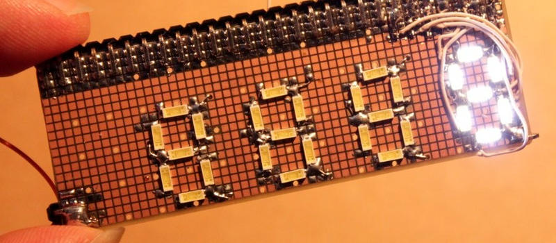
[Yann]’s DYPLED entry into this year’s Hackaday Prize isn’t very useful to most people. It’s a tiny module that connects to a 16-bit parallel bus, and displays a hexadecimal number on a few LEDs. It’s useful if you’re diagnosing a problem on a computer from 1982, but just barely. The real wonder here is how [Yann] is doing this cheaply and easily using some weird techniques and strange parts.
The display for this tiny device is an array of 36 LEDs, arranged into a set of five seven-segment displays. Homebrew seven-segment displays are cool, but how is he driving it? Not with a microcontroller, that’s for sure. Instead, [Yann] is using an old trick of using parallel memory to store the patterns of the seven-segment displays. This parallel memory comes in the form of a two megabit Flash chip, with the data inputs tied to the 16-bit input on the board and the data outputs connected directly to the LEDs. It’s a brute force approach, but it works.
There are a few additional features for this tiny board, including a switch to display a 16-bit bus in hexadecimal or decimal, signed or unsigned, and a pot to change how bright the LEDs are. The most amazing part is how [Yann] managed to fit all of this on a very, very small PCB. Most of that trick is due to using a thin, small TSSOP package for the Flash memory, but fitting this circuit onto a two layer board is amazing work, and a great entry for the Hackaday Prize.


I think you mean the address inputs not the data inputs being tied to the board inputs. The data bus is tied to the segments of the display, and the address bus would be tied to the board inputs and the patterns for the segments is stored in the flash at the addresses corresponding to the inputs of the board. Essentially a flash look-up table.
Not quite grokking the full mechanics of his way or your way. But there’s a way of treating an memory chip kinda like logic, you send the digital numeric value in as the address and get out the data pattern that lights the corresponding LEDs on the data lines… I think that’s what you’re saying right?
You pretty much have it…
The address lines are the inputs, and the data lines are the outputs. Any arbitrary output can be mapped to any arbitrary input. The up side is that ANY combinatorial logic can be designed, and the timing is very predictable. The down side is that you waste a LOT of gates this way for something with a wide input. In this case, to handle two digits you need 16 inputs and 14 outputs. That means almost a MILLION bits of memory (917,504 to be exact). That means a LOT of transistors. On the other hand, you can do the same thing probably using a couple of dozen gates of discrete logic. So, yeah, for wide inputs, this is not exactly efficient. However, if you happen to have a memory just lying around…
In fact, this trick, in miniature form, is used as the basis of logic in most FPGA families. A logic block will typically include a tiny memory with something on the order of five inputs and three outputs. However, instead of calling them a memory, they call them a “LUT” (look-up table). In the case of 5 inputs, 3 outputs, that makes only 96 bits of memory, a much more manageable size. The size of the memory needed is (2^(number of inputs)) x (number_of_output), so each bit of input will double the memory.
Actually, to clarify here, my numbers were wrong. A hex-to-7-segment uses four bits input and 7 bits output per digit. This means that 16 bits of input would need 28 bits of output. On the other hand, assuming a 16-bit wide memory, you only need 8 bits of input, and 14 of the output bits.
You’ll find on the schematic that the memory being used has separate data inputs and outputs. The display is connected to the memory outputs, not the input or address pins.
Using the memory as a lookup table containing basically the truth tables for the 7segment displays is fine on its own.
But i think the clock generation is the real gem in this.
I understand that its some sort of rc circuit but the inverters and diodes confuse me :-|
Looks like a relaxation oscillator? But it’s drawn weirdly/gates are backwards. The diode thing is so that you can dial charge vs discharge current with the pot.
Hah ! well I’m not the original author of this oscillator !
Look at @K.C. Lee’s #Charleplex Xmas Tree without uC : https://hackaday.io/project/8416
I added the diodes and trimpot for PWM, I tested the circuit on breadboard to get it right, then miniaturized it.
Logic operations can be represented by lookup tables, who knew?!!
;-)
Nice work.
I call this pre-computing because some other computer does the processing and stores the results for the dumb(er) electronics to function.
I remember seeing a JAMMA arcade game board and assuming the the second stacked board was missing. On closer examination I could so no connectors for a second board. It was an amazingly detailed tile based scrolling game and had no CPU just many ROMs, some latches to hold simple variables and some de-bounce circuitry to buffer the controls onto an internal bus. Even the sound was in ROM.
Now I am wondering if this method could be used to allow a lowly 8-bitter uC to do (or lookup) complex robot kinematics by pre-computation.