Printed circuit boards are a fundamental part of both of commercial electronic equipment and of the projects we feature here on Hackaday. Many of us have made our own, whether done so from first principles with a tank of etchant, or sent off as a set of Gerbers to a PCB fab house.
To say that the subject of today’s Retrotechtacular is the manufacture of printed circuit boards might seem odd, because there is nothing archaic about a PCB, they’re very much still with us. But the film below the break is a fascinating look at the process from two angles, both for what it tells us about how they are still manufactured, and how they were manufactured in 1969 when it was made.
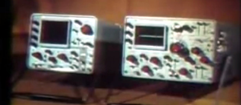
Tektronix were as famous for the manufacturer of particularly high quality oscilloscopes back then as they are now. The Tektronix ‘scopes of the late 1960s featured several printed circuit boards carrying solid-state electronics, and were manufactured to an extremely high standard. The film follows the manufacturing process from initial PCB layout to assembled board, with plenty of detail of all production processes.
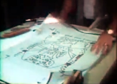
In 2017 you would start a PCB design in a CAD package, but in 1969 the was incredibly manual. Everything was transcribed by hand from a paper schematic to transparent film. Paper mock-ups of component footprints four times larger than actual size are placed on a grid, and conductors drawn in pencil on an overlaid piece of tracing paper. Then the pads and pattern of tracks are laid out using black transfers and tape on sheets of film over the tracing paper, one each for top and bottom of the board. A photographic process reduces them to production size onto film, from which they can be exposed and etched in the same way that you would in 2017.
Most of the physical process of creating a PCB has not changed significantly since 1969. We are shown the through-plating and gold plating processes in detail, then the etching and silkscreening processes, before seeing component installation and finally wave soldering.
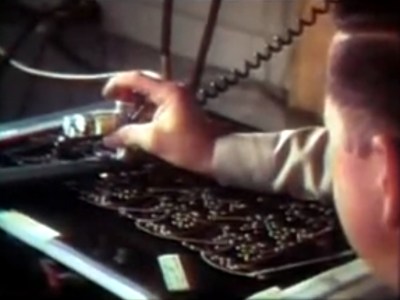
What are anachronistic though are some of the machines, and the parts now robotised that were done in 1969 by hand. The PCB drilling is done by hand with a pantograph drill for small runs, but for large ones a fascinating numerically-controlled drilling rig is used, controlled by punched tape without a computer in sight. Component placement is all by hand, and the commentator remarks that it may one day be done by machine.
The film remains simultaneously an interesting look at PCB production and a fascinating snapshot of 1960s manufacturing. It’s probable that many of the Tek ‘scopes made on that line are still with us, they’re certainly familiar to look at from our experience at radio rallies.
Thanks [Macona] for the tip.


Video in 240p is an atrocity. The original was most probably a chemical film without a such insane resolution limitation, even after decades of archiving.
Depending on the stock a lot of 60s stuff was at risk of catastrophic deterioration bythe 90s so it either got put on analog video tape or primitively digitised then.
Here is another Tektronix video from 1968, about the birds and the bees and the flowers and the oscilloscopes. Seems to be higher quality: https://archive.org/details/oscilloscopesandtransducers
Doesn’t the narrator sound like Richard Anderson ? (recently passed away) aka “Oscar Goldman” from The Six Million Dollar Man. He did voice work for Shell Oil around the approximate time of this film. So wonder if he did this one for Tek ?
Funny, his voice immediately reminded me of Bud Haggart’s (in)famous Turbo Encabulator spoof: https://www.youtube.com/watch?v=Ac7G7xOG2Ag
The thing that strikes me about this is they did their printed circuit boards in the house? At what point and why did Techtronics decide to start outsourcing their circuitboard production?
Everyone did PCBs in-house back then. Business to business collaboration was rare as businesses were completely independent.
The in-house manufacturing capabilities at Tektronix were astounding. Remember the real magic of their scopes back then was in the CRT itself. These guys were making 1Ghz realtime analog scopes in the early 1960’s. From exotic CRTs & later hybrid circuits, down to the chassis and knobs, they made it all in-house.
They were accepting competitive bids for PCB production while I was working there, but I think 95% of the boards I saw were marked “T1”, which indicated in-house. This was 1980-84. Why? Not a clue.
I should also mention, that Tek didn’t always manufacture everything themselves. I always thought that they made all of their own CRTs, but I have a Tek 321A from the late 1960s that has a CRT by General Atomics.
oh that’s interesting, yeah I assumed all but the earliest monolithic 500s had Tek CRTs. I think my 514 has a Dumont CRT?
Yes, I’ve seen Dumonts in 500-series ‘scopes, too. Oh – correction, it was a General Atronics CRT in the 321A.
I like these retro videos, thanks for posting it.
I also like those 60’s era curvy traces. I am wondering if there is any easy way to get a CAD tool to make such things.
DipTrace has curvy traces, others probably too. I used them in a simple headphones amp to make it a bit more interesting…
TopoR makes boards like this:
https://en.wikipedia.org/wiki/TopoR#/media/File:Topor_board.jpg
Wow, I have that exact Type 453 scope at 28:27 on my bench right now! It’s awesome.
nice! me too! It’s one of my daily drivers… mostly to work on other oscilloscopes with ;)
I used to buy >>>=ARCHER=> branded tapes and pads from Tandy and do boards this way in the 70’s. Well I just used tapes and pads and etch. No plating.
I was interning in the mid 70’s at a place that made electro-optical instrumentation, and one of the first tasks that I had was proofing PCB artwork against the mylar film layouts. Fixing errors was kind of painful.
Yes, it was sooo time consuming that it was easy to justify checking it over two or three times, as painful as that was.
I have re-visited some of the old techniques like wire wrap but I will leave the tapes and pads alone, I think lol.
Like every other electronics enthusiast, I wrote several primitive PCB CAD programs on the earliest computers that could support graphics. They were next to useless of-course as we only had dot-matrix printers back then. Though they did make a good guide for the manual process and they were easy to store on FDD.
I have used wire wrap semi-recently. Most of the modern parts are some variety of SMT though, so I just go straight to PCB for most of my prototyping.
I used to use the Tango PCB package, and through the years built up a huge set of libraries. I still miss the simplicity of that program. It runs just fine in a DOSBOX window under Linux. I miss a lot of the parts that I used to have in the Tango system. Slowly, I have been adding the stuff that I am using currently to the libraries on my current CAD package. My graphical programming skills were not up to that kind of work before I got a smoking deal on the Tango Schematic and PCB packages.
I used wire-wrap as a bit of nostalgia. My modern replacement for point to point wire-wrap is you put a number of small CPLDs on boards and use then to rout signals.
I have a hundred or two of Xilinx XC9536XL as they are excellent for this and with their 0.8mm pin spacing they are easy to solder.
When I was younger, wire-wrap gave me a cramp in the wrist. Now it gives me a cramp in the brain lol.
One interesting thing though (I’ll try and find a pic) is that everyday pin headers are excellent for wire-wrap and they let you use the board with the chips up instead of chips down.
https://cdn.hackaday.io/images/6495531461474430682.jpg
Yup, that is the way they did it back then. Wish I had a buck for everyone I fixed. Have a 454 on my bench to this day. Built in the 60s, but to the best of my knowledge still on export controlled list (over 100MHz).
Just a suggestion: I’d change this phrase- “…but in 1969 the was incredibly manual…”, to “…but in 1969 this was entirely manual…”.
Do we have programs that can automatically place components? Autoroute, yeah, sorta. But auto place? I think technically components are still placed by hand…
Yes, you can automatically place components in DipTrace, TopoR, and other software. Their autorouters also work well on layouts that simpler routers (for example EAGLE) will fail on.
I think “component placement” in the article meant physically populating the PCB (see the section with the narrator’s line “in the future, a machine will replace many of these hand operations” starting at 24:45 in the video.) It was done entirely by hand back then whereas today with SMD components it’s commonly done by pick-and-place machines.
I had several occasions to speak with the Chief Scientist Emeritus of Textronix Morris Engleson in the late 90s and mid 2000s. Very cool person he survived the Holocaust as a boy by his father establishing a debt to a Polish farmer for rent and hiding based only on his promise which he later paid after the war. A brilliant person, but we never talked scopes, we only ever edged around spectrum analysis and I arranged him giving a lecture about encoding data onto a wireless signal.
https://www.youtube.com/watch?v=l7EJHrfiqWc
OK, terrible quality and gets cut off near the start, too bad was a good tech shmooze.
That’s pretty cool that they used a negative of the trace as a resist, plated more copper and then gold, and used the more inert gold as the etching resist. I’m so accustomed to the old school hand played out or toner transfer methods of ferric chloride etch processes. I’d have never thought to expose the traces, and cover the area to etch and do it that way.
The other benefit is that the original copper is very thin and requires very little etch to be removed. Far less chemical waste.
Definitely! That’s gotta also significantly speed up mass production too.
I’m pretty sure a “dilling machine” is something entirely different…
Anybody remember laying out double sided PCBs using double-scale “rubylith” tapes? Red tape for one side, blue for the other, both laid out on one piece of transparent plastic for design simplicity and to ensure registration. The photographic reduction and exposure was done using corresponding red/blue light to separate the planes.
I had a technician doing that for me in the very early 80s; once he had put a track down, he refused to lift it! CAD was a godsend.
I think rubylith refers only to red film.
Bishop Graphics (incorporated 1965?) was the major supplier of black tape and film images of IC layouts, and later introduced the red and blue tapes which greatly improved the ease, speed, and accuracy of the layout process for 2 layer PCBs.
For anyone interested here is a link to the Tektronix online museum. http://vintagetek.org/
Why do most of these old technical films look like they were transferred to video from film through a lens smeared with petroleum jelly. Also, you can easily see horrible pixelation. When were these converted to digital?
1) The originals was never good to start with as they were often PAL or NTSC or even worse – film which degrades rapidly
2) After years of archiving on old analogue media such as VHS/BETA VCR the quality degraded further
3) Modern digital codecs are extremely poor with low resolution degraded video
“Pantograph dilling machine uses a manually moved styuls on a template to drill six boards”
that should probably be pantograph drilling. Great article though
Quite right, fixed!