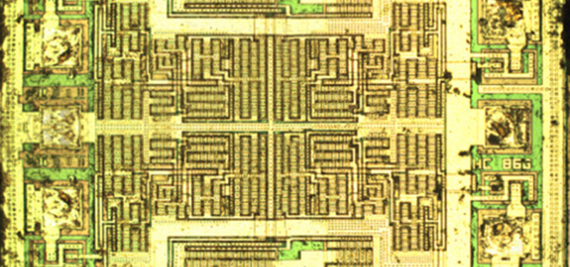
A few semesters back, [Jordan] was in an Intro to Hardware Security course at CMU. The final project was open ended, and where some students chose projects like implementing a crypto algorithm or designing something on an FPGA, [Jordan] decided to do something a little more ambitious. He wanted to decapsulate and reverse engineer an IC. No, this isn’t taking a peek at billions of transistors — [Jordan] chose a 74-series Quad XOR for this project — but it does show what goes into reverse engineering silicon, and how even simple chips can be maddeningly confusing.
The first step to reverse engineering a chip is decapsulation, and for this [Jordan] had two options. He could drop acid, or he could attack a ceramic package with an endmill. While hot nitric acid is effective and fun, it is a bit scary, so [Jordan] mounted a few chips in a 3D printed holder wedged in the vice on his mill. By slowly bringing the Z axis down a few thou at a time, he was able to find the tiny 1 mm square bit of silicon embedded in this chip. With the help of a grad student and the cleanroom, this square of sand was imaged with a very nice microscope.
Now that [Jordan] had an image of the silicon itself, he had to reverse engineer the chip. You might think that with less than a dozen transistors in there, designing an XOR out of transistors is something anyone with a bit of Minecraft experience can do. This line of thinking proved to be a trap. Technically, this wasn’t an XOR gate. It was a transmission gate XNOR gate with a big inverter on the output. Logically, it’s the same, but when it comes to silicon fabrication, the transmission gate XNORs aren’t able to sink or source a lot of current. By designing the chip as an XNOR with an inverter, the chip designers were able to design a simple chip that could still meet the spec.
While [Jordan] managed to reverse engineer the chip, this was quite possibly the simplest chip he could reverse engineer. The Quad XOR is just the same silicon repeated four times, anyway. This is the baseline for all efforts to reverse engineer silicon, and there were still a few confusing traps.


“While hot nitric acid is effective and fun, it is a bit scary, so [Jordan] mounted a few chips in a 3D printed holder wedged in the vice on his mill. ”
Aw come on, it’s just an eyebrow. :-D
I used to work at a company that had equipment for decaping chips. The plants near the fume hood exhaust were dead! And, at first, management didn’t see the need for an eye wash station!
I’m more worried about what kind of environmental regulations would allow a company to not scrub their nitrogen oxides before pumping them into the atmosphere.
It’s all fun and games until someone looses an eye… :-)
And then its just fun :D
I’m kind of amazed that he was able to expose a die embedded in resin by milling away at the chip. I’d think that unlike with a ceramic package, a plastic package would have no void in it for the chip. That’s why I use hot sulfuric acid to dissolve the plastic. I’d rate the difficulty of getting a usable die using milling at 9/10, hot sulfuric acid at 2/10, fuming nitric at 1/10. In terms of danger, milling gets 1/10, hot sulfuric gets 4/10, nitric gets 6/10. As for expense, which includes time, milling 6/10, sulfuric 3/10, nitric 4/10.
I use nitric and/or sulfuric depending on the target but never considered milling for the same reasons you mentioned. This is not a practical approach to reverse engineering silicon.
He should have just used a chisel to split the package at the seam.
“transmission gate XNORs aren’t able to sink or source a lot of current. By designing the chip as an XNOR with an inverter, the chip designers were able to design a simple chip that could still meet the spec”
That line doesn’t make much sense to me. Perhaps the first XNOR was meant to be XOR?
Nice job Jordan !!
I believe the description is correct.
The overall chip function is an XOR
This is such old technology well known to chip designers, I don’t think I am giving away any chip design secrets in the text that follows…
As mentioned in the article – It is made up from an XNOR followed by an invert buffer stage. Logically this is an XOR but the invert can be up-sized to provide decent drive capability and the XNOR can be small. This is smaller in area than a massive single stage XOR gate, and has lower input capacitance (as mentioned) and large drive with perhaps a little extra transport delay due to the multi stage construction. Having a single gate stack (single transistor) between the output and the power or ground is good in the invert buffer stage vs compound logic stacking.(google body effect for why)
The other reason is the double invert buffer is used is to provide gain to sharpen up slow input slew rates. A slow ramp the internal nodes B’ and B” leads to ugly behavior ( logical fail in the case of transmission gate flops) BTW, The schematic should have B, B’ and B”, the same name on a schematic implies connectivity). This is often used on flip flop clock inputs to transmission gate flip flops. similarly and/nor can be constructed from different multi-stage logic rather than a single stage gate.
There are other ways to create XOR in transmission gate style logic, some with keepers or ouput feedback. Each option has pro/con to be considered by the chip designer.
On larger chips we may use un-buffered transmission style logic , latches, flops, muxes too, or even just pass gate style for area/performance/power reasons, sometimes with built in latching function, but only where we can carefully control the input rise times(Slew rates) and output loading. It is easy to mess up.
Often these old chips were designed for easy modification to other logical functions, just by modifying some of the metal connectivity . We could make one chip and spin several variants very quickly. So don’t be surprised if you see some extra transistors in there that don’t make sense or are not even fully connected. It is probably for a different variant of the chip.
I hate when people draw crappy schematics without showing the actual interconnects. Instead they rely on signal names for connections (and in this case, colored dots).
Had Jordan draw the actual schematic interconnects he might have realized that he’s cross conneced those input inverters (which in this design doesn’t make sense).
He correctly identified that this is a transmission gate XOR, which is a common design. Transmission gates are fast, but as they lack restoring drive, so need a level restoring stage (in this case, the final inverting buffer).
A XOR composed of separate *conventional* CMOS gates would require more transistors, and based on the propagation delay through a series of stages, would likely be slower.
more transistors, more chip area, slower
vs.
fewer transistors, smaller, faster.
Transmission gates rock!
Be aware that almost always, when the internal gate level schematic or a chip is shown, it’s a simplified version that is LOGICALLY correct. The actual transistor level implementation can vary substantially.
The article explains that the technology used for the gate itself couldn’t give too much current, so they built it as the opposite and added a powerful NOT gate at the end, thus transforming a weak XNOR into a powerful XOR.
I read it as the inverter was doing all the heavy current lifting and the XNOR just signaling it to do so
I’m not EE, so this one confuses me a bit: “The transmission gate XNOR requires two inputs and their complements. I expected to find two inverters on the inputs, but I found four! It turns out TI was inverting once to get the signal complements, and inverting that to get the original signal back.”
Wouldn’t you expect 6 inverters then? (Or are 2 eliminated by the difference between pFET and nFET gates at the transmission gate?)
Already got it. Actually the schematic explains it once you “get” the color codes ar labels.
74-series means TTL, but the device analyzed is CMOS
Yeah, it’s an 74HC (cmos) series IC.
The device is a SN74HC86N which technically is 74-series, but it’s of the 74HC high-speed CMOS subfamily instead of the 7400 TTL family.
You can definitely see your skills in the work you write. The sector hopes for even more passionate writers such as you who are not afraid to say how they believe. At all times go after your heart.