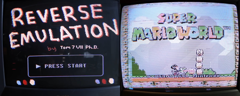
This is a stellar hack, folks. [Tom7] pulled off both full-motion video and running a Super Nintendo game on a regular old Nintendo with one very cute trick. And he gives his presentation of how he did it on the Nintendo itself — Nintendo Power(point)! The “whats” and the “hows” are explained over the course of two videos, also embedded below.
In the first, he shows it all off and gives you the overview. It’s as simple as this: Nintendo systems store 8×8 pixel blocks of graphics for games on their ROM cartridges, and the running program pulls these up and displays them. If you’re not constrained to have these blocks stored in ROM, say if you replaced the cartridge with a Raspberry Pi, you could send your own graphics to be displayed.
He demos a video of a familiar red-haired English soul-pop singer by doing just that — every time through the display loop, the “constant” image block is recalculated by the Raspberry Pi to make a video. And then he ups the ante, emulating an SNES on the Pi, playing a game that could never have been played on an NES in emulation, and sending the graphics block by block back to the Nintendo. Sweet!
The second video talks about how he pulled this off in detail. We especially liked his approach to an epic hack: spend at least a day trying to prove that it’s impossible, and when you’ve eliminated all of the serious show-stoppers, you know that there’s a good chance that it’ll work. Then, get to work. We also learned that there were capacitors that looked identical to resistors used in mid-80s Japan.
These are long videos, and the first one ends with some wild speculation about how a similar human-brain augmentation could take a similar approach, replacing our “memories” with computed data on the fly. (Wait, what?!? But a cool idea, nonetheless.) There’s also another theme running through the first video about humor, but frankly we didn’t get the joke. Or maybe we just don’t know what’s funny. Comments?
None of that matters. A SNES game was played in an NES by pushing modified graphics from a “ROM” cartridge in real-time. And that’s awesome!
If you want more Nintendo-in-Nintendo goodness, check out this NES ROM that’s also a zip file that contains its own source code. If you compile the source, you get the zip file, which if you unzip gives you the source to compile. Right?
Thanks to everyone who sent this in to the tip line! [darkspr1te], [Erik S], [Reversnes], [Tim Trzepacz], [KAN], [Jorhlok], and [Qes]. (Did I forget anyone?!?)


Doesn’t seem to emulate any SNES sound at this stage. He speculates it is possible though. The “joke” about humor was awfully technical but a generally fair point about certain subtypes of humor. Though it was extremely specific and required the viewer to follow several key points to “get” their joke. Which wasn’t a joke so much as a series of low level explanations about why and how this is funny and why this fits into that schema of humor, which it actually somewhat does.
The presentation format of doing this on an actual NES was amusing. Wonder how long it took to create / convert all of the low resolution graphics to make this presentation. Let alone how long it took to explore and put this hack together. This wasn’t a weekend project.
The last part of that one presentation video got awfully speculative though I do follow the concept of what they are referring to. It still remains to be seen how that actually manifests and there is significant technical work to be done before that’s relevant anyway. At least it didn’t go into brain uploading and other such stuff. It did seem somewhat tangential and incongruent compared to the rest of the presentation though in terms of subject matter though given the subject matter is a reverse inception style microcontroller assisted rom hack, it’s not exactly like it is wildly off base given this isn’t exactly a technically light achievement and the Venn diagram of people who are technically able to pull this off and who speculate at a deep level about future technologies probably overlaps considerably.
Lastly, curious why the validation chip can’t be easily emulated? It’s just easier to harvest one?
The functionality of the lockout chip can be easily emulated, many homebrew carts sold today handle it that way. You can do it with an attiny if you want (https://forums.nesdev.com/viewtopic.php?f=9&t=9797). I imagine for a one off project it was just simpler to grab one from an existing cart or perhaps he was just unaware, but I find that unlikely.
I assumed it was easily emulated at this point. Mostly curious why he decided to drop one in rather than emulate it (presumably directly through the Raspberry Pi)? I agree, it seems to be much easier for the one off to just drop a chip in rather than add an Attiny13 or recompile things. Might also be a performance consideration? He had to move to a “quad core” Raspberry Pi to have enough horsepower and even after doing so, timing on some of the signals is already surprisingly tight as it is.
IANAL, but bypassing copy protection would be a crime under DMCA, and even speculating about the level of difficulty of doing it could probably be construed as providing support to lawbreakers.
The chip in question doesn’t perform anything to control access to the copyrighted data in the cartridge.
It is (or was) a custom chip provided by Nintendo to indicate your cart has a license to run on the NES. Completely different IP laws.
But the real world fact of the matter is, legal or not, who wants to defend against a lawsuit by Nintendo?
Remember, this is the same company that claims emulating a 6502 CPU they didn’t create is in violation of Nintendo copyrights. Note, the emulator, we’re not talking about the game ROMs which are copyrighted. They have stated and attempted to press charges in the past for running your own home made code that you own the copyright on, under a 6502 CPU emulator.
That is the type of twisted logic, on top of gobs of money to spend on lawyers, one would need to deal with to prove you aren’t doing anything illegal. Who needs that mess in their life? Best to not risk it even when you are in the right.
NES doesn’t use an off the shelf 6502. It uses a custom 6502 that they do own the rights to. Games coded to run on a stock 6502 aren’t going to run on Nintendo’s 6502.
Just do it and hope they don’t notice/care.Is there not some sort of insurance you can take out? or just say it was for research or a ‘work of art’
Getting sound out of it would require a modification to the NES itself. Existing flash carts use one of the unused pins to send analog audio, which the console has to wire in to get mixed with the audio output.
Also, kind of curious that they knew enough about the NES platform to basically build the most high-powered mapper ever, but didn’t know how to build a CIC stun circuit (or use a free CIC implementation like the AVR one).
I don’t think it’s so much about not knowing rather than not wanting there. Clearly, the guy knows how the heck the NES works.
By the way, anyone who’s looking to know how the heck the NES works can go to http://wiki.nesdev.com/w/index.php/NES_reference_guide and access the knowledge humbly shared over the years by the community, and their great work of reverse-engineering and documenting every technical aspect of the console to the last detail (including the *totally* predictable PPU’s logic sequential operations), organized in a nice wiki on which many NES tinkerer have been glad to rely. Many thanks to them for that invaluable resource, because most people don’t have infused knowledge about everything like this “genius”.
Mind blown
Nothing new here, this sort of thing was actually done in real games for some cartridge-based systems back in the day. That doesn’t stop it from being neat though.
Care to elaborate? I do not believe any commercial game ever used anything like this…
Virtua Racing for the Sega Genesis had a co-processor in the cartridge.
I fail to see how co-processor chip like the super-fx and the one used in Virtua Racing are anywhere like what this guy is doing…
Starfox and Super Mario World 2: Yoshi’s island both had the Super FX chip in them, this was a RISC CPU functioning as a GPU, handling 2D and 3D effects. It’s a 21MHz chip compared to the 3.58MHz main chip. So this fits the bill.
Not the same thing.
You have to go back to the early 1980s, the Famicom was launched in Japan in 1983. Particularly, the price of RAM around 1983 (high!).
The NES used the same sort of tile-mapped design as most arcade machines did. It’s a lot like character-mapped modes on a computer or terminal. The screen is 256×240 pixels, with around 10 colours on screen at once. You could store all of this in just 2k. How?
Well, compression! Sort-of! The screen is stored as a grid of blocks, a lot like how JPEG and the like works. Many blocks will contain the same data (in fact they HAVE to, there isn’t enough memory for each one to be different). Each block can have a palette of 4 colours, chosen from so-many possible palettes, chosen from the 52 colours the hardware can possibly generate.
Without going all the way into it, stuff like that. Pointers to pointers to pointers, lots of referencing, lets you store full-screen very vital, colourful graphics, animated fast, with a tiny bit of RAM and not too much CPU power needed. If it were done the way graphics are done now, as a bitmap, you’d need something like 16K or 64K RAM just to store it, and there’d be so much data to shift, you’d hardly be able to move more than 1 tiny sprite at a time.
While there was 2K RAM to store the screen as tables, the actual blocks were stored in ROM, on each cart, on it’s own bus. The ROM for graphics blocks (CHR) and 6502 code (PRG) were separate, on separate address and data busses, accessed separately. CHR ROM could be, using on-cart bank-switching (called a “mapper” chip), as big as you liked, games could have any number of enormous levels if you could afford the ROM chips.
Anyway later, more sophisticated games didn’t have to use CHR ROM for pre-defined graphical blocks to build a screen from. They could use RAM instead. Thus giving true bitmapped graphics, at the cost of a bit of complexity. Wasn’t used much, but was possible. Of course the system was fundamentally fairly simple, so most things were possible.
And THAT is what this does! At least I think so! The Pi fills in the CHR blocks in real-time, updating them as it wishes. You don’t actually need ANY code running on the NES’s 6502 at all! It could just be displaying a “static” screen, for all it knows. The Pi can change the CHR blocks as it goes, but the NES CPU doesn’t need to know about that. In fact that’s how I’d implement this. Then add a bit of code to read the NES’s pad, send the results back to the Pi, and you have a basic Pi-NES that can do anything. With a bit of a filter, you could fairly straightforwardly get Doom running on there, or X server or whatever.
This is different from the Super-FX chip and the similar Sega thing, because they ran code on the console that sent requests to the on-cart co-processor. In this case, the console is largely just a higgledy-piggledy frame buffer, doing almost no work at all. In Super-FX games, the SNES is in charge. In this case, the NES is just a pipe between the Pi and the TV screen.
This is exactly what the Super Game Boy does, it captures VRAM data from the hardware on the cart and pipes it as CHR data to the host machine through an interface chip.
Now I want to see a stock NES running a Doom (or Quake) cartridge! Should be possible, albeit without sound.
It’s a mapper. An extremely complicated and elaborate one that adds pretty unique functionality, but still the same basic idea of just about every Famicom/NES game beyond the simplest ones.
Mapper chips are a great idea. Just bankswitching really. Atari 2600 games used a simple 7400 chip, something like a quad-nand or NOR or the like, to trigger theirs. 2K of the 4K ROM space the machine could see, would be paged, live, upon accessing (even reading) a particular address, ie by putting address $xxxx on the bus.
Of course PC and all the other registers and hardware / CPU states were still chugging along on the assumption the old ROM was there. But it wasn’t. It just meant programmers had to be careful, and had to know exactly where which byte ended up in the finished product.
There were even more complex mappers (or bank-switching schemes as everyone else calls them) on later games with more ROM and even RAM.
But Nintendo topped the lot, for it’s day, with it’s complex mappers on the NES, carried away pretty quickly to the SNES. Makes me wonder why they just didn’t design the SNES right in the first place. Keep the bank-switching in the machine, or else bring the right address pins out and use a CPU with enough pins in the first place. Meh, Japanese!
What NES game “injected” sprites directly into the NES by bypassing the typical topography of the cartridge ROM and instead bypassed that using it’s own hardware on the cartridge? It’s physically possible (though with more modern hardware that was not made or economical back then) and some SNES cartridges did some functionality by physically building it into the cartridge hardware (the Super FX chip was a dedicated hardware coprocessor on the Graphics Support Unit on the cartridge) but nothing like this hardware based video injection method existed in a commercial cartridge as far as I am aware. Camerica did a “piggyback on an official cartridge” method but that was only to bypass the lockout chip.
I’m 99% sure the NES was the only Nintendo cart to suck it’s graphics directly from the cart to the graphics chip, as the picture is being drawn, bypassing the CPU altogether. I’m pretty sure the SNES and GB had on-console RAM to hold their graphics blocks instead, so stuff would all be stored in one big cart ROM, graphics and code together, with the code copying graphical data to the graphics chip at the programmer’s will.
That, and the SNES had a few different graphics modes, including a bitmap, also stored purely in RAM.
So this is only possible on a NES.
I’ve sort of been meaning to do something similar for a couple years now, just never had the time to dive in. I’m glad someone has already done a lot of the ground work for this!
Kudos, this is dope!
The human-brain augmentation idea reminded me of the movie “Flight of the navigator” in which a boy’s brain gets filled with alien information and then the alien later says “Correction, I need the superior information in your inferior brain”
throughout the video, what the heck is that glitching on the screen? (lines of the spirtes, hyphens, whatever) ..is he (wirelessly) transmitting dirty ntsc RF or is the NES fouled-up or is his hacking to blame? (sorry if my question is answered in the vid, i’m hard of hearing and inattentive to detail.) [i’ll not ask about the low-quality TV/monitor used in the presentation; perhaps it was free.]
nevermind. ‘noise and jank’ is explained @~12m52s
First off! Amazing demo. Great technical details and amazing documentation. Seriously well done!
Long time reader here, but very occasional commenter. I’m a little late to the party here, but figured I’d throw a guess in here. I don’t know if this is the entirety of it, but I’d wager that its a good chunk of it. You really can’t (read: shouldn’t) use a Cortex-A (*especially* a multi-core one) to try and reproduce tight electrical timings like this. I don’t use the Raspberry Pi since there’s basically no way to product-ize the end solution but the reasons below should hold true. There are several reasons why this won’t ever achieve the 100% glitch-free solution but it does provide an excellent learning opportunity as to why.
1) A Cortex-A processor like the A7 or A53 in the Raspberry Pi is running Linux is going to run the majority of its code out of external DRAM. While this has an extremely high bandwidth, for the needs of the project, it does have a non-zero and variable latency associated with it. The data also comes in using bursts and can’t be quickly randomly accessed like SRAM can. Any time that code is going to execute that hasn’t been run recently it must first be read out of DRAM and stashed into an internal SRAM cache on the processor. After this initial CPU stall to fetch code the CPU can then can then resume code execution at full speed. This typically gets done on either the L1 or L2 cache (L2 cache is required for multi-core processors). I haven’t looked, but it’s common to have a random eviction policy on the cache memory (there’s only so much of it) so any code that hasn’t executed recently is going to get kicked out pretty quickly if you’re running an OS like Linux on the CPU core at the same time.
That’s a lot of technical details, but you can summarize it best by saying that any code that hasn’t executed super recently on a full CPU like this one is going to take a small, but randomized extra burst of time to execute. Since the TV signal out of the NES draws from the left to right and all of the glitches on the video tend to burst on the left side I think it’s safe to say that the Raspberry Pi isn’t keeping up with outputting graphics for the start of most lines because the memory isn’t local and fast yet on the CPU core doing the work.
2) A multi-core processor like this is going to be even worse in the same regard because any processor accessing the DRAM to fetch code/use memory ties it up for an extra amount of time. So having the emulator and OS running on CPU cores 2-4 is going to drive up DRAM usage which will further aggravate the issues highlighted in #1 above.
3) Additionally (and I haven’t looked this up for the Raspberry Pi) most CPUs will have a single internal bus that’s used to access CPU registers. So if you have one CPU that’s reading a timer peripheral, SD card, GPIO, I2C, etc it can potentially block out access by another CPU core for a few clock cycles. This probably isn’t amounting to much, but if you have 1 CPU core sitting in a loop polling for a hardware event to complete you could potentially take up ~50% of the internal bus bandwidth that the other cores get what’s left depending on the CPU priority assignments.
4) A Linux system like this running on a Cortex-A core is going to require use of the MMU (Memory Management Unit). This is the semi-magical hardware block that allows dynamic memory located in non-contiguous, random DRAM outside of the processor to appear as any memory address without any holes in it. It’s used for making programs all think they begin at address 0 (or equivalent) as well as malloc() (or equivalent). This magic comes at a cost though. There are normally 1-2 tables of memory that take a pointer or memory address and translate it “into the real world” -> AKA logical-to-physical translation of addresses. This tables don’t normally fit into the SRAM on a processor so they’ll live in DRAM also. Therefore it’s possible that to read the DRAM in #1 & #2 above that it could take up to 3 DRAM reads to fetch a single byte of memory out of DRAM. This makes the problem worse.
Most of the above can be tweaked/improved on the existing platform but it’d be a lot of work and I still don’t know as it’d be 100% perfect. Alright, enough of my speculation. If I was to go about trying to improve upon this my suggestion to fix the graphical glitches is that I’d change the Raspberry Pi out for a BeagleBone Black. You lose 3/4 of the CPU cores for the emulator which are serious overkill already but get 2x 200MHz single-cycle embedded microcontrollers instead (Programmable Real-Time Units = PRU). These cores each have a small internal SRAM for their code and a few small SRAM memory pools to use for data. They have access to DMA which means that anything the CPU can do can be piped into/out of the PRU at high speed (but paying the latency and time-uncertainty mentioned above once per transaction).
Since these PRUs are selected on CPU pins using the GPIO feature Mux instead of having the CPU’s internal bus shared between 3 processors there’s zero uncertainty about how long it takes the data to get to the outside world. Simply write to the parallel output register and 2 clock cycles later and the data exists to the outside world.
These PRUs + single 1GHz processors are incredibly popular for CNC equipment where they can drive a reliable signal output without errors. You really want to have the same thing here.
There was a similar hack for the Vectrex a while back. I don’t have the original post with a digitized “Bad Apple” video but the gist of it was an outboard PIC32 does all the heavy lifting to generate the display list then feeds that info to the Vectrex via dual-port RAM. This project evolved into the Vectrex32.
https://hackaday.com/2017/04/12/32-bit-processing-for-the-vectrex-arcade-system/
cool
He basically made a 32X for the NES… or a more proper term would perhaps be a 16X, either way good job dude! Now I must top this by building a 128X for the N64.
“Hit Deborah cliff over the head with a hole”…
i’d explain but it’s way too NSFW andor i’ll tell u when ur older ;)