One of the big problems with doing PCB layout is finding a suitable footprint for the components you want to use. Most tools have some library although — of course — some are better than others. You can often get by with using some generic footprint, too. That’s not handy for schematic layout, though, because you’ll have to remember what pin goes where. But if you can’t find what you are looking for SnapEDA is an interesting source of components available for many different layout tools. What really caught our eye though was a relatively new service they have that uses computer vision and OCR to generate schematic symbols directly from a data sheet. You can see it work in the video below.
The service seems to be tied to parts the database already knows about. and has a known footprint available. As you’ll see in the video, it will dig up the datasheet and let you select the pin table inside. The system does OCR on that part of the datasheet, lets you modify the result, and add anything that it missed.
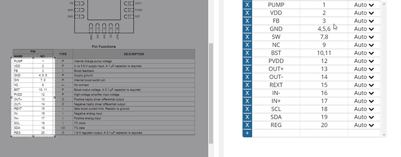
This is undeniably cool, although once the wow factor wears off you realize that you still have to locate the table and set the pin types. Their demo shows how you might have to add other things like a ground pad, too. For a small part like the one in the demo. it wasn’t much easier than just typing the data into a table. A giant part might have more benefit.
Of course, once you have a symbol, you can get it for many popular software packages including Eagle, KiCAD, OrCAD and many others. You might worry about people creating bad symbols, but they’ve thought of that. When you create a symbol like this, it is only visible to your account. So if you mess anything up, you’ll only affect your own projects.
Probably the most attractive thing about this — even if you don’t build your own footprint — is how you can get parts for a variety of layout programs. When we looked at layout tools, that was the first thing you had to do was make a new symbol and footprint.


I wonder how it does with connectors? I can never find pin 1.
We don’t yet support connectors, but the main database at http://www.snapeda.com has a lot of ready-to-use connectors created via our collaborations with connector vendors in the industry. Everything is free and there are no limits since we work with the vendors directly to make this data available. Hope that helps!
It would be so much easier if manufacturers would commit to publishing this data in a computer-readable format. Why hasn’t some industry association forced this yet? Yes, there are standard footprints, but only some parts fit in those packages. What’s missing is a standard WAY of describing NONstandard footprints…
I’m not sure if this is what you’re looking for, and it’s a bit messy but it works, Ultra Librarian is an application that attempts to bring libraries to most of the popular design packages. I’ve mainly used it to import microchip PIC microcontrollers into Eagle with varying degrees of success. It often is quicker to design the footprint yourself, with the symbol and footprint just the way you want it.
FYI, you can convert Ultra Librarian BXL files to pcb-rnd, gEDA PCB and Kicad compatible parts with:
https://github.com/erichVK5/BXL2text
How do the big names deal with it?
Just going to put this here :)
https://xkcd.com/927/
well even after signing up and probably ending up on a newslitter list, i cannot really evaluate this feature with anything other than the 3 examples provided. looks fun, but it doesn’t even tell me what i’m supposed to do (pricing information is no help either) to be able to use it. so yeah. fail.
Great feedback Luke! SnapEDA is used by over 100,000 registered engineers and it’s completely free! This feature (InstaBuild) is a free feature that shows up on any parts that have tables in the datasheets for which we already have a verified footprint. We’ll take your feedback into account to expand it more broadly to more components. Thanks again!
update:
loading https://www.snapeda.com/instabuild/start/ lets you upload any datasheet.
i did so with the chipone ICN2053 datasheet and selected the pin table which led to a terrible and utterly useless mess.
to be fair, there’s a watermark across it. so i tested again with the TLC5957 datasheet, where it wasn’t as bad, but for example “IREF” got recognized as “[REF”. no es bueno.
what a waste :D
Thanks Luke! Computer vision & OCR is not yet perfect so we’re a bit limited there, but we have some ideas to improve it. Thank you for flagging this – I will make sure to let our engineering team know.
Nah, your naive implementation sucks :(. Lacks domain knowledge, or even common sense.
Do you really expect pin label be more likely to include non alphanumeric symbols? Not to mention you should have a database of standard technical pin designations, like “iref” “iout” “vref” etc, to instrument OCR.
even https://norvig.com/spell-correct.html was >10 years ago.
>“IREF” got recognized as “[REF”
Usually its a case of [ classification being few % above I. Something like OCR ending up with [ at 85%, I at 82%, and L at 45%, and then going for that 3% instead of common sense :(
In real world [ isnt even that usual to show up without closing ].
Not to mention you could have OCR generate uncertainty map, and let user know with a light color highlight over borderline choices – more friendly than silent errors making them painstakingly check everything by hand.
Great feedback thanks! This is a beta feature so glad we caught this opportunity to improve it now. I will send this info to our engineers so we can improve it further. You rock!
I find most footprints out of SnapEDA don’t work directly without significant changes, which require me to look at the DS and then check everything. By that time it would be quicker to just create myself so at least I know it’s correct.
Nice idea but no banana.
Hi there! I’m curious when the last time you tried it was? We’ve made drastic improvements to the database over the years since we started the company, and continually make improvements. Would love to know which part(s) you have downloaded and we will investigate asap. If you’d be open to it, I’d love for you to email me at natasha@snapeda.com your username and I can investigate. Thanks a lot!
Drawing parts is a simple task that for some reason tends to scare away the noobs. I also used to search the internets for the parts I needed. But it takes 10 minutes to define a new part+package in most cases, and you can be sure about your design.
I once had to draw the footprint for a QFP100 and only after ordering the PCBs we noticed that my design was not centered correctly and the contacts on opposite sides were off by half a unit. This would have been an expensive mistake, but luckily the company doing the soldering for us found a workaround by mounting the chips with a tiny bit of rotation.
Well at least you could only blame yourself. Imagine if it was a random downloaded footprint that was wrong.
I find designing footprints for new parts the most time consuming chore in electronics design and It is great that SnapEDA are at least trying to resolve this issue. I think that a lot of the issue is to do with the software used for the schematic capture and PCB layout. Kicad has a pretty good user interface and creating packages is fairly simple. Eagle is also reasonable. I haven’t had much experience with Altium or Orcad so I cannot comment. I currently have to use Easy-PC and am finding it to be the most frustrating experience of my professional career! Sharing footprints is exceedingly helpful there. Unfortunately Easy-PC seems to be one of the least used software packages ever…
I really enjoy the Altium IPC footprint wizard for creating the PCB/foorprint layout – But makeing an 250pin fpga schematic part takes forever :(
+1 on the Altium IPC footprint wizard. Works really well most of the time, and i really love that it generates the STEP files of the package for 3D rendering from all the package data you feed it.
Altium has the great feature that you can copy and paste the pin and pad position from Excel. I have used this method a lot by creating a list of pins and coordinates in Excel, sourcing the pin names and numbers from the manufacturer’s website; that way FPGAs are a breeze to create.
I recently moved job and switched to Kicad, and I find that frustrating, but I’m finding ways around it
“The service seems to be tied to parts the database already knows about.”
Then how do you know it’s really using OCR? Maybe the database was just pre-populated.
As an engineer involved, I can tell you that the feature uses OpenCV. The feature shows up on pages where we don’t already have a symbol to provide engineers an alternative method to build them.
Copy your pin numbers/names from the data sheet PDF.
Edit the component from the Libraries Panel.
Then In the SCHLIB List panel:
Right click and select Smartgrid Insert.
Close the window and your component will have the pins added.
This was supposed to be a reply to Martin E
I just signed up and 2 min later I was creating my first part (DS1882).
Although i really like KiCAD, I find the library management and part creation quite confusing for new or occasional users.
I hope this service helps me creating my own PCBs more quickly and without searching the internet :)
Glad to hear you were able to get started. Let us know if you run into any issues along the way. This is a beta feature on SnapEDA so we’re very open to ways to improve it to make parts creation easier.
@Natasha keep up the good work. I really like where SnapEDA is taking component creation.
We’ve used SnapEDA extensively on our latest PCB design. It’s a fantastic tool, and this vision technique would certainly be a great addition!
Some of the comments here, though they are valid, are put very abrasively. I’m glad that [Natasha] in particular is being very positive about them.