For the first in a series of posts describing how to make a PCB, we’re going with Eagle. Eagle CAD has been around since the days of DOS, and has received numerous updates over the years. Until KiCad started getting good a few years ago, Eagle CAD was the de facto standard PCB design software for hobbyist projects. Sparkfun uses it, Adafruit uses it, and Dangerous Prototypes uses it. The reason for Eagle’s dominance in a market where people don’t want to pay for software is the free, non-commercial and educational licenses. These free licenses give you the ability to build a board big enough and complex enough for 90% of hobbyist projects.
Of course, it should be mentioned that Eagle was recently acquired by Autodesk. The free licenses will remain, and right now, it seems obvious Eagle will become Autodesk’s pro-level circuit and board design software.
Personally, I learned PCB design on Eagle. After a few years, I quickly learned how limited even the professional version of Eagle was. At that point, the only option was to learn KiCad. Now that Eagle is in the hands of Autodesk, and I am very confident Eagle is about to get really, really good, I no longer have the desire to learn KiCad.
With the introduction out of the way, let’s get down to making a PCB in Eagle.
The Eagle Overview
There are three main parts to Eagle. A board is exactly what you think it is. The board describes the layout of components, holes, pads, connections, traces, and mechanical design of a printed circuit board. In the most general sense, the board is what you send off to a fab house to get your PCBs made.
The schematic is not a board design file and is not sent to the fab house. The schematic is the description of all the components in a circuit, and how they’re connected together.
The libraries in Eagle describe each and every part used in a project. Each part in a library has two components, a package, and a symbol. The package is a one-to-one physical representation of the part used when designing the board. The symbol is an abstraction of the part, used when designing the schematic. The package and symbol are combined into a device.
The reason for combining packages and symbols into a device is yet another abstraction; you can get the same microcontroller cores in different packaging — the ATtiny85 we’re working with in this article comes in both SMD and through-hole packages. Because we can combine different packages and symbols together, we do not need to duplicate work by making the ATtiny85 symbol multiple times. Likewise, if we’re designing a lot of parts that all have an 8-pin DIP package, we can reuse that package multiple times.
Building A Library
 The first step for all these tutorials will always be designing a part, in our case, a DIP-8 ATtiny85. To do this, we’re going to open Eagle and create a new library. Save your library, give it a memorable name, and check out a few buttons on the toolbar:
 This is the Symbol button, used to create new symbols
![]() This is the Package button, used to create new packages (footprints)
This is the Package button, used to create new packages (footprints)
![]() This is the Device button, used to combine symbols and packages into a single device.
This is the Device button, used to combine symbols and packages into a single device.
The first step for all these tutorials will always be designing a part, in our case, an DIP-8 ATtiny85. To do this, we’re going to open Eagle and create a new library. Click on the Package button, name a new package ‘DIP8’, and continue on to the package editor.
Making the package
This is the package editor. There are only three relevant buttons on the left-hand toolbar we need to use.
![]() This is the ‘Pad’ tool. You use this to create through-holes for each pin in your part.
This is the ‘Pad’ tool. You use this to create through-holes for each pin in your part.
![]() This is the ‘Line’ tool. Use this to draw an outline of the package. This outline will eventually become the silkscreen on the PCB.
This is the ‘Line’ tool. Use this to draw an outline of the package. This outline will eventually become the silkscreen on the PCB.
![]() This button, above the left-hand toolbar, is the ‘grid’ button. This is used to set the distances between each line of the grid in the editor, and therefore how pads and lines snap into place.
This button, above the left-hand toolbar, is the ‘grid’ button. This is used to set the distances between each line of the grid in the editor, and therefore how pads and lines snap into place.
The DIP8 package is simple enough — it’s just two rows of four pins, 0.1″ on center, 0.3″ between rows. Draw a few lines to outline the chip, place the pads according to the ATtiny85 datasheet, and the package is almost done.
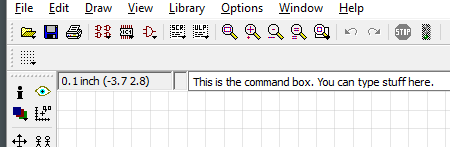 To avoid confusion when combining the package and device, we’re going to name the pads. Eagle still has the vestiges of an old DOS program, and a lot of the commands are accessed by typing a command into the box right above the editor. Type ‘name’ into that box, and click on a pin. We’re going to name each individual pin according to how they’re usually numbered.
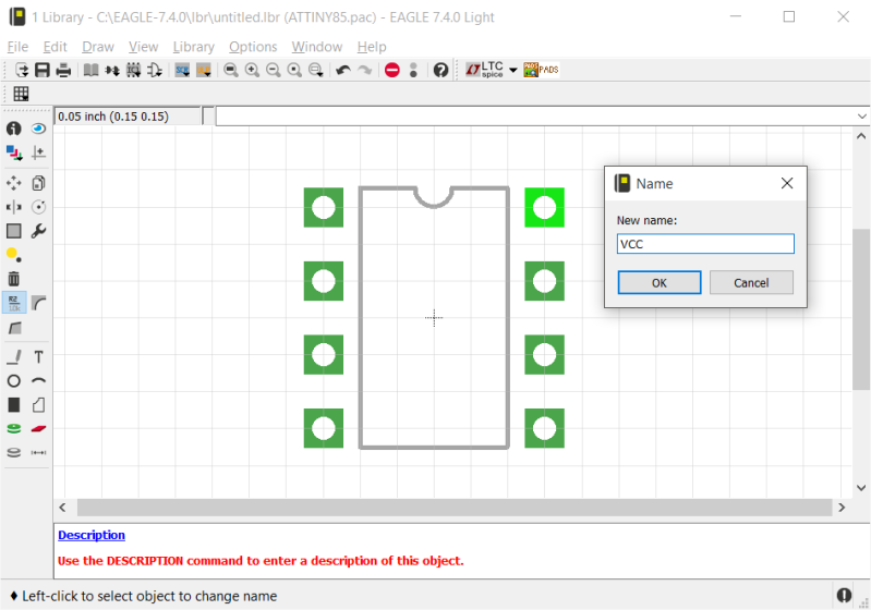
With that, save your library, and click on the ‘symbol’ button to create a schematic symbol for this chip. Name the new symbol ATtiny85.
Making a symbol
The symbol is what you will place on your schematic. It defines the electrical connections of the part in your schematic, but unlike the package, it is an abstraction. You could place pins anywhere. In fact, it’s a good idea to lay out your package so it will be easier to draw the schematic.
Just like designing the package, we really only need two buttons on the left-hand toolbar. We use the ‘line’ command to draw a box, and the ‘pin’ button to place pins. These pins are what we use in the schematic to connect parts together. Draw a box and place eight pins around the perimeter, two on one side, and six on the other (it’s common in microcontroller symbols to place power on the left and GPIO on the right like this).
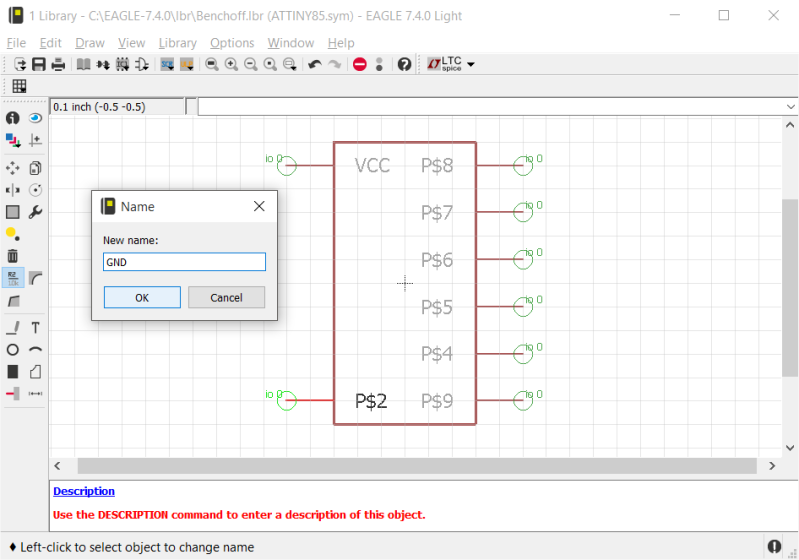
When that’s done, type ‘name’ into the command box, and start labeling your pins. We’re keeping power and ground on one side, so name the top one ‘VCC’ and the bottom ‘GND’. On the other side, label each pin ‘PB0’ to ‘PB4’, making the last pin ‘Reset’.
Save. Now we can combine these two parts into a single package.
Combining the Package and Symbol into a Device
 Create a new device, and click the ‘Add’ button in the left-hand toolbar. There’s only one symbol in your library right now, so click that, and drop it on the editor.
Now, we’ll need to select the package this symbol goes with. At the bottom of the window, click the ‘New’ button. Again, there’s only one package in your library, so click it.
Now, we have a window with the symbol in one window, the package in another, and we need to connect the pins in the symbol to the pads in the package. The obvious button to choose is ‘Connect’.
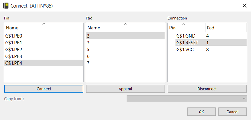
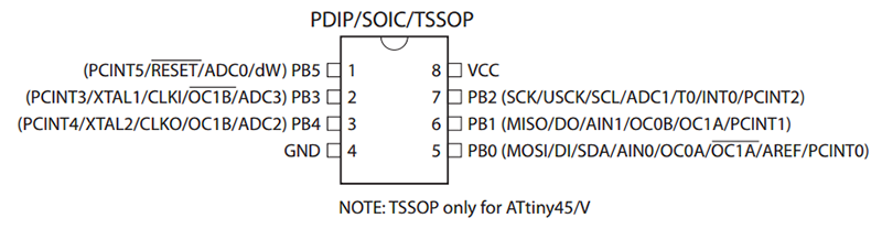
Read the datasheet for the ATtiny85, and make sure all the pins are connected to the correct pads. For the ATtiny85, VCC should be pin 8, Reset should be pin 1, and GND should be pin 4. Connect the rest of the pins to the rest of the pads. When all the pins are connected, hit OK, and save your library.
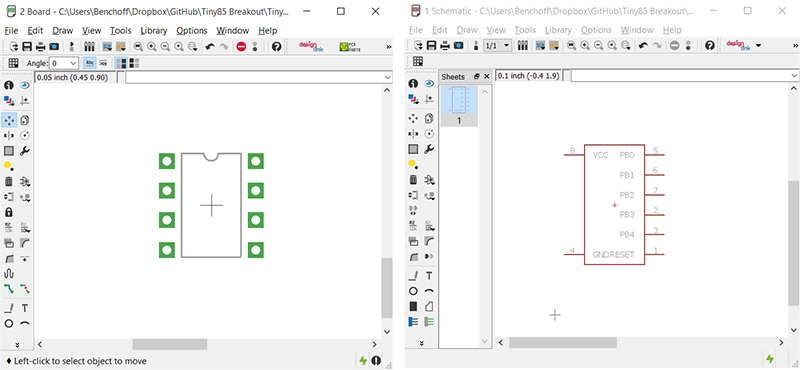
The ATtiny85 is a small and simple part, but that’s all it takes to create any part in Eagle. To test it out, go to the Eagle Control Panel, create a new schematic, and add a part. Select the library you just created, and place the ATtiny85 device. From the File menu, select ‘Switch to Board’ and you’ll see something like this:
This is not a complete guide to doing everything in Eagle. Even this part of the tutorial did not cover creating labels, text, or anything except the bare minimum of making a part in Eagle. That’s the hardest part of building a PCB in Eagle, and in the next part of this tutorial, we’ll dig into plopping all the parts for our board down on the schematic, nudging them around on the board, and drawing traces between them.
That’s all you need to do to create a single part in Eagle. The next post in this series will go over putting this part in a schematic, creating a board, and sending that file off to a fab. As with all posts in this Creating A PCB in Everything series, we’re looking for suggestions on what to do next. If you have a favorite EDA design tool, leave a note in the comments and we might get around to doing a tutorial for that piece of software.


Okay, but there are already numerous device descriptors freely available online so I don’t have to re-invent the wheel for every resistor, capacitor, IC, connector, etc. I wish to use, Right?
True, but learning at the beginning how to, saves the grief later when you have to.
I second this. Also, as you go, copy symbols from well-known libraries (Sparkfun, Adafruit, Microbuilder, etc.) into your own library. Being at the mercy of other libraries sucks in the long run, and can lead to inconsistencies in your layout that make your board look crappy. Having a nice collection of known good packages to choose from is pretty sweet.
Yes, and there’s already an ATtiny85 in the default Eagle libraries.
You don’t know how to use Eagle unless you know how to make a part, though. Since I’m doing all of these ‘making a PCB’ things with the same circuit, I need to demonstrate how to make a ‘tiny85.
I’ll make more sense in a few months.
Agree with your point of view. I’ve seen many people stuck in their designs for not being able to find a correct footprint/symbol available. The creation of symbols and footprints is the first and most important barrier to be brought down when learning any CAD for designing PCBs.
I can say by experience that designing new components both in Eagle and Kicad are very easy, although I got more cards in my sleeve when designing the components in Eagle, mainly because the time I’ve spend learning how to draw lines and position pads using the scripting language, which result in precise footprints.
Last bit of advice, after designing a component (even when using one form a third party library), print it 1:1 on paper and check if it fits as expected.
Trust that many libraries from Element14 and the web have countless flaws.
This has sabotaged several student’s board designs over the years.
(some parts are only out of spec by 0.5mm, and so a paper print out to scale will not show the issue.)
Adafruit and Sparkfun libraries from github are the only ones checked by numerous users, but still get the odd bad part.
Take the 1 hour to do your custom parts, or use KiCAD that seems to be complex enough to exclude the jokers trying to do pad layouts with a tape measure.
Autodesk has not really improved any product they owned since the 1990s.
=/
Yes, I see your point(s) about learning how to make your own descriptor i.e. Device, but to design a resistor instead of plucking out a axial 1.2 Kohm 1/4 Watt 20% tolerance film resistor when there is (hopefully) a decent one available to use.
But I was unaware, that repositories would have faulty devices listed…
Sometimes the footprints might not designed for your PCB flow or if you want custom ones. e.g. toner transfer, milling or even PCB fab. Some fab might not like to mill a lot and you’ll need a round pins.
You are putting a lot of faith on someone. I have seen enough of badly made (bad metric to imperial conversion, truncation), wrong footprints and ugly symbols. It take a lot less effort to make a footprint than to fix a wrong PCB after it is made.
Well, I personally have create a “passive library” which hold all kind of pasive components.
1) all footprints are the same (0805 for capacitor, led and resistor are the same, save for silkscreen)
2) somewhat ajusted to my stock
3) added informations (1K resistor ? 4 footprints from 0402 to 1206, power indicated for each
0) (the most important) I added ATRIBUTES to my components.
So, now that I create a board, each time I place a single resistor, I know that I have it in stock, and with the help of a single script, I can have the exact price of my board, kind of component by kind of components, and a RS/Farnell/Mouser command list if needed (I even estimated PCB price from surface).
That’s the point of using your own libraries : automation (eg time saving and mistakes preventer)
When developing Open Hardware it is a good practice to use an Open Source software, then KiCAD is better option.
Sure, you believe Autodesk will improve Eagle, but it couldn’t happen. Hackaday is an influential hacking web site and it should be nice to see more people here encouraging to use KiCAD not complaining you are too lazy to learn it. Sorry, but this is the third time I hear you saying it, this time I cannot hear silent!
Agreed, I definitely think HaD is the place to introduce open source, cross platform, parametric CAD, such as the excellent KiCAD, an not to promote a free, but so limited proprietary software.
Fully agree.
Agreed +1. But not just for the sake of being open source. KiCAD is the better product. Not yet in terms of features and usability but in terms of the outlook. Also, commercial software has to generate profit of some sort. This needs to be taken into consideration. Eagle is not developed for free. The developers are being payed from something. “If it’s free, you are part of the product.” Might be OK, just be aware of it.
Also, will Eagle be owned by Autodesk next year? Will it have active development next year?
Brian, it’s like finally switching from Windows 7 to Linux and then you switch from Linux to Windows 10. This doesn’t make sense.
“Not yet in terms of features and usability”
Push and Shove router THIS RULES
Parts and symbols being separate while it makes the eagle crowd complaint, it’s a nice thing to have.
Differential pairs and track length tuning
32 layers of unrestricted size
They are beginning to implement a simulator
Basic functions are more important than what you mentioned: Assigning nets in pcbnew; back annotation; changing nets on pins (sometimes impossible in OpenGL mode). Inconsistency of usage in different modes. Measuring of distances too complicated. Setting origin of coordinates too complicated (just as simple as “set origin of coordinates to center of footprint or trace). Moving in x-direction xor y-direction not possible with mouse. Gerber plot underdeveloped (how to assign what goes in what file). Classes underdeveloped. Insufficient possibilities to control and vary solder mask. In the footprint editor: Only lines where there should be rectangles. Unnecessary restrictions that seem to be implemented on purpose (eg. what I can do on a copper layer). As if the program tries to protect me from me doing what I want… as if the program knows better than I do but in fact it doesn’t.
I admit, for some of my arguments, I don’t know what eagle currently can or cannot do. But this is what I expect from a good, usable pcb tool.
TBH: some of your arguments are valid. Others, the solution is so insanely easy. And in many ways BETTER.
Others are a different in outlook of the workflow. Yeah I agree forward and back annotation would be nice, but not always what I want anyway. In some cases I’m glad it doesn’t do that.
Measurement? So damn easy its trivial and weird you mention it as aan issue. No one else has ever mentioned it.. click the measure tool. Click start point. Click end point. Done. Granted it will only place measurements on documentation layers.
Quick visualsxare easy too.. mouse to a start point hit space bar. That is now zero-zero. Go to another point, read x-y at the bottom.
@MRE:
back annotation doesn’t have to be active continuously, but why are you sometimes glad, that the option isn’t there at all?
Regarding measuring distances: How do I measure something very basic like the shortest distance (space) between two traces (depends on position, thickness and angle)? How do I even measure the distance between the centers of two traces or between the centers of two pads, if those are offgrid (eg because I HAVE to work with different grids)? For the seconds question, sometimes pressing “x” helps. Sometimes it doesn’t.
Sometimes you have to have different grids for making a single footprint (pain with kicad). Sometimes you want to connect pads from footprints with different grids… It’s not that the continuous drc in kicad is such a nice thing to have. It’s more like that you are forced to rely on it.
I recognized that using space has some function. But it reminds me of counting pixels in a bitmap viewer rather than what I expect from a pcb tool.
Might want to do you own tutorials and submit to HaD instead of going off off topic talking about your non-Eagle PCB tool?
These are the dumbest set of arguments HaD has had in a while. That’s actually a difficult thing here.
Congrats.
OSHW people are so silly. I picture them in high-water skinny jeans, lumbersexual facial trimmings, and Cassy Naggat glasses. They’re spouting their ideals while hypocritically paying a big margin for Apple/Google/Samsung/Starbucks/etc brand identity created using slave labor.
OSHW and sustainable business models only coexist if there is zero innovation. e.g. Sparkfun and Adafruit.
I’m choosing to learn KiCad over Eagle in large part it’s open source but I don’t think you would say that about me. I certainly don’t believe it is wrong to pay for software. I write closed source for-money software for a living!
I’ve been taking my time to make my choice of EDA, reading a lot of internet comments, watching Youtube videos about it, etc… One thing I have noticed is that there are a lot of Eagle users out there who are very invested in that product. EDA is hard and these suites have a lot of features and tricks to learn. So many people review KiCad and say it is good but adapting is too hard after years of using Eagle.
Eagle’s free version has been available for a long time and is available today. Sure, it’s limitations aren’t that bad for a hobbyist level user. I doubt I would ever hit the layer count limit. I might some day hit the board size limit but I could always just split onto two boards. Those limitations do exist however and with KiCad they never will. With no years of Eagle baggage why chose it?
Further.. what if one day free Eagle is not available? Don’t get me wrong, I’m not entirely opposed to paying for a product. I’m not expecting an affordable non-free version of Eagle though. Well.. not without a student id anyway. I’ve never seen an EDA product that was priced for hobbyists. They are all marketing to real EEs. Companies have much bigger expense accounts. I know there are lots of people here wtih multi-thousands of dollars invested in Altium and stuff like that but that’s because they are professionals. If I bought one of those my next expense would be for a divorce attorney!
Of course Eagle could change in other sorts of ways besides altogether eliminating the free version. The limitations on the free version could get worse. They could drop Linux support.(or OSX for those who actually like that) They could merge into Circuit Maker forcing everyone to store all their designs on the cloud. It could just slowly lose popularity until finally development gets canceled some day years from now. Sure, If any of these happen I could go on using an old version forever. Eventually though I would be stuck on an old OS, old hardware and lose compatibility with everyone else on the internet.
All of these things may be unlikely. They are not however impossible. I would be much more surprised to see this with KiCad. I’m not saying that Open Source guarantees software will have a future. There has been plenty of stuff that never really hit critical mass and disappears after a year or two. After a certain point though if the developers drop it or take it in a bad direction there will always be someone to fork it. Just look at Star/Open/Libre Office! I think KiCad is there now.
So anyway.. tldr.. I’m not an idealogical hippie about open source software but I do see free and open as advantages. I’d pick a for money piece of software if the price was reasonable and it’s advantages in other areas outweighs the oss advantages enough to be worth the money. As more oss matures however, the areas for doing so become slimmer and slimmer. I’m glad the products I work on are non-technical niche products that are unlikely to ever have OSS competition!
I totally understand why someone with years of Eagle experience would stick with Eagle for now. There is always going to be a price for doing so though, monetary or in limitations. Some day it will probably not be worth it. For me it’s not about beards, hipster glasses and overpriced coffee. It’s just about making a safer, longer term investment of my time and effort.
good read. thank you for the time that must have taken.
hmmm that sounds sarcastic, but its not!
Funnily enough, I cancelled my download of Eagle and downloaded KiCAD because of “Show me a[n] OSHW company.”‘s snarky comment.
Thank you acassis for keeping me in-line!
Designing your own parts is nesecary evil.
You also know what you have.
For the small i make I try and use the same parts in all my designs so that 1 limits my inventory and keeps my library small and manageable.
Try finding a ready made 1/4 W through hole resistor in the eagle library. – yes they are there but now exactly which foot print do you need to use?
it’s quicker to draw your own.
“but now exactly which foot print do you need to use?”
Umm, according to my junk box, about 11 different ones.
Do Circuit Maker!!!
Why? Ask Altium for a Circuit Maker tutorial since they are making profit from you using the tool.
Hope you include DesignSpark PCB in this review roundup!!
As somebody who has never seen this or any PCB software before and actually wanting a tutorial you need to dumb it down a bit. You lost me at “Combining the Symbol and Package”. How and where to “create a device” isn’t clear and no “add” button seems to appear anywhere. Pretend we’ve never seen this software before, because those of us that want and need the tutorial likely haven’t.
Bitching aside, thanks for this tutorial. I have a couple of projects I want to design and build on more than just a proto board and was literally about to go looking for software and a tutorial but dropped in on HAD yesterday to find my prayers answered.
Is no one going to mention schematicpal.com ?
I have been using Eagle since 1995 and have made hundreds of 2 and 4 layer boards. It is missing a few things (signal propagation simulation – and easy export to 3d modeling software) but over all it rocks.
Has anyone here ever used auto-trax DEX ? I bought a license for really cheap – and it looked to be way better than eagle – but I could never find the motivation to learn it. Anyone here use it?
Oh, it pains me to write to complain (because I’m not usually one to complain about your articles), but where did you get the idea to make this series? You seem to be completely unwilling (you even say so) to learn how to use the other programs for designing PCBs out there, yet have the audacity to make a series on how to use these programs to make PCBs.
I don’t think that’s a good idea. We’ll probably be treated to numerous counts of “this doesn’t work like Eagle, it’s so confusing!” in the remainder of the series with you failing to use the other programs correctly because they follow differing UI and workflow philosophies.Which is a shame.
I’ve started PCB design with Eagle, but heard about KiCad and wanted to try it out before it became so massively popular (long before the CERN involvement), and was absolutely blown away by it. I’ve used Eagle and KiCad in parallel for a few months, before switching entirely to KiCad. KiCad may have its drawbacks, but the fact alone that Eagle will not prevent you from violating design rule constraints while you work is completely unacceptable for any kind of serious work where I find it important to focus on routing and not on trying to think about clearances.
” find it important to focus on routing and not on trying to think about clearances.” That’s what “snap to grid” is for…
For the crudest designs, true.
Automating the clearance is invaluable once you experience it.
Oh Brown Pinchoff. So silly.
Commenting on the differences between programs BEFORE you have become proficient in all of them is like explaining Trumps political platform. You have no clue and it might be completely different tomorrow.
I’m looking forward to your KiCad article.
I started with Eagle long time ago, when there was no KiCad available. I used it for years when I discovered Kicad, and KiCad was just the better tool, for me it was obvious from the beginning that it will be the way to go for me. Sure there are concepts which are different, but different != bad. Of cause it is a afford to get into a new software but it also opens some doors to new views on the way.
After all KiCad is free, which means there are no artificial limits to motivate you to buy “the real ting”. I understand that they have to earn money, but for the user it leads to problems.
What if you need to interchange connections 3&4 on a 5 pin 0.1″ header and you use KiCAD? Go to sch editor, do it, generate netlist, read it in pcbnew and start routing again…. It is a PITA. In eagle ,interchange in sch editor and the change is annotated into the pcb editor. The eagle way is too easy than stopping the flow of routing in KiCAD to do the ‘netlist’ . I like KiCAD , but the ease of switching back and forth in sch editor and pcb editor in eagle stops me using KiCAD. My question is to KiCAD community that, are the developers going to build this into KiCAD?
In Altium it’s even easier.
What are you talking about? KiCad supports Forward Annotation: http://docs.kicad-pcb.org/stable/en/getting_started_in_kicad.html#forward-annotation-in-kicad
While it is not as quick&fance as the back-and-forward of the Eagle windows, there’s no need to re-route the parts that are already done…
11 steps vs one step
I don’t need to say which is easy,do I?
I felt exactly the same way !!! when I played with Kicad this made me imediatly hate it, but I was “sure” that i was just missing something obvious – I thought that there was NO WAY that in 2016 a “modern” CAD package would not automatically back-anotate – after all Eagle has been doing this since the early 90’s.
Sadly this is what the large paid CAD world do.
Those commercial packages usually has a much higher licensing fees for the layout/routers, so the mortal engineers are not encourage to fool around. There are some advantage to splitting a design into two *non-integrated* programs. e.g. a large project where Bob is working on schematic full time while Pete is kept busy working on a few other layout projects.
For one man shop or casual project, this is a bit of a pain. It feels clunky like using an elephant gun to kill a fly. a FOSS package should consider an alternate flow for simpler projects (like 90+%).
That model of Bob and Pete works great if Pete is smart enough to “see” that the .1 uf cap tied to the vcc net near U1 in the schematic must be physically close to U1 in the lay out. The huge problem with having the engineer “just do the schematic” is tha the design intention is lost at the point that the stupid cad program exports a wholly insufficient netlist (as opposed to a netlist that contains layout geometry)
My office does this – we have a “layout guy” and we use Orcad (worst most expensive schmatic tool ever) that outputs a netlist that layout guy pulls into pads-pcb. This entire exercise is an example of how to fail and spend lots of money .
Using eagle, and actually doing placement while desiging the schematic, I am able to do in four layers what most people do in 16 .
I am really curious why auto-trax DEX has little market share. Has no one else here seen it?
Most of the contractors I have deal elsewhere have been around long enough to know enough about high speed circuits and decoupling caps. We have length constraints for termination, topology so they can’t mess up those without trying.
Someone changed the power supply layout *after* I checked and okay in a review. He changed a very high current track into a thin track to make space for a test point. Unfortunately didn’t catch it. I had to sit down with him and explain to him why it was a bad idea – from a design and from a process point of view.
As much as I like the control, I don’t think I want to handle the layout on these boards. We have the layout people come in on 3 shifts to do the place/routing which took about a month or so just on that project. The board was very big and was pushing Cadence’s limit, and they actually build a larger version for us.
For my own projects, I use Eagle. I don’t care if XYZ Cad is free range gluten free, asbestos free etc. I don’t listen to vegans to tell me what to eat.
No. That little obstacle is put there to teach you to finish your design before you start routing.
I don’t want to be taught by a bad teacher. Is KiCAD supposed to be a pcb tool or is it some sort of learning software?
Even If your design is finished, you cant tell if the connections N$45 and N$6 will intersect each other or there is a trace blocking a connection just by looking at the complete and ERC passed schematic.
(sidenote:I have nothing with Einstein)
No edit on hackaday.
*(sidenote:……)* was not ment to be posted on HaD.
I admit to making a sniffy comment, don’t take it to seriously. Of course it’s nice to pin optimize when working on your own project. In a larger project however, where such a change request has to go through three departments to get approved by all intermediate bosses, it’s moot to even ask. It is always better to fail EMC testing.
And yes, I am growing bitter and cynical.
Or, just the device doesn’t work as it was a high speed clock line which had a trip around the world and a lot of inductance. Let’s hope they find this error after millions of dollars wasted and learn something, as you said.
If the routing was not meant to be done with cleverness and PCB design constraints as feasibility of design, no one would have continued developing manual methods to route if having AutoRoute
I was working for a defense company at one point, the changes in schematic are tracked and revisioned via the release process. I can see it a pain for making a sensible layout. I do however try to take the pin orientation into consideration by sketching out the signal paths. Engineers have no access to the limited layout licenses and layout is more hands off kind of thing.
At other places where the whole schematic/layout are concurrent and we can interrupt and work with layout person without corporate level of BS, I still try to get a feel on the layout to make life easier. Getting an idea of signal paths etc up front is also useful for SI simulation and reduce the amount of back and forth.
I wrote program that translate the component foot print library into window meta file format so that I can import them and play with the layout. I also wrote a program that highlights the different type of signals for BGA – power, I/O, clocks whatever by matching the signal names.
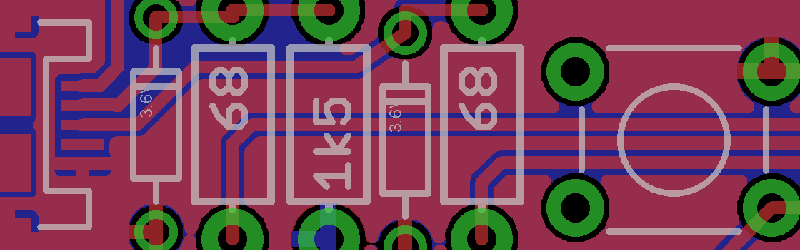
Please use also grid when routing your PCB please. The picture is one of the ugliest routed pcb I’ve seen.
Screw the grid, keep inductance low. When I get a design for review and see components in neat little rows and columns I know it will be crap.
those weird angles won’t help with that either.
All the components in neat rows seems to be a standard for most PCB I’ve seen..
…only on PCBs designed by true craftsmen. The rest of the world thinks “who cares, it doesn’t matter anyway”. I happen to disagree.
Good article! It’s often quicker to create or adapt existing parts (be sure to lookup how to copy parts from one library to another) than finding suitable parts on the net. I own a very old collection of parts that don’t have any matching footprints. I also created often used connectors as a separate part like a PICKIT3 5 pin connector, an LCD16x2 connector without the unused data lines etc.
I also moved a lot of common parts (resistor, capacitor, crystals, oscillators etc) to my own library so I don’t have to hunt through the many libraries, and the search tool isn’t always helpful either.
Also check, double check and recheck all parts with more than 2 pins in the downloadable libraries, it may well be that the pins are mirrored. I’ve been caught out on quite a few occasions assuming the transistor, potmeter or IC footprints are correct while they’re not. My guess to the cause of this is that some datasheets present the part in an ambiguous way, not stating if the view is from the bottom or the top, front or the back. Also remember that Eagle shows the board from the component (through hole) side (tracks in red = top side). If SMDs are placed on the top (red tracks) and you move them to the bottom, make sure you check the footprints, they should be mirrored compared to the top tracks. It’s usually easier to delete the part and pick the part that’s already on the correct layer/side.
And be careful when soldering, eagle shows the blue tracks through the board, but the actual pcb you will flip over for soldering, so everything is mirrored! You can’t print the PCB with the board design mirrored while the labels are not, this can confuse matters if you want to place components. I usually print to PDF, load it in Illustrator, use multitranslate to flip all text labels and print at 3x the normal size to make it easier placing the components.
I usually place a label near the first pin of all components on the top and/or bottom layer, print it and place the components on the paper to check if the orientation and pins are correct.
Also use the junction feature. If you don’t, some nets may not connect properly, creating orphaned nets that don’t get power or signals.
And before you even start learning Eagle, assign all the toolbar icons to logical keyboard shortcuts! It will save you many extra clicks, moving back and forth between menu’s and toolbar and drawing area. This needs to be done for each mode: schematic, symbol, footprint and PCB drawing. It’s best to setup similar functions like move to the same shortcut.
And finally there are some very good tutorials on youtube, and on some webpages as well. Great for learning how to actually use all these functions.
If you mirror the component (sending it from the top to the bottom layer) all the signals are still connected the right way. All the routing done will give messy results and may violate the DRC. No need to make a separate part in your library for bottom parts. It will be confusing and errorprone.
Oh and never trust shady part libraries floating around internet and actually print the footprint 1:1 on paper and place the component on top. Some other tips I’ve posted: http://smdprutser.nl/blog/things-to-avoid-when-sending-pcbs-to-the-fab-house/
I also did some posts on how to fix common errors made on PCB: http://smdprutser.nl/blog/fixing-late-night-pcb-design-errors-adding-pullups/ and http://smdprutser.nl/blog/fixing-late-night-pcb-design-errors-swapping-bussignals/
True, if you assume all transistors are the triangular B C E, you’re going to have a baaaad time.
well i am trained as a computer engineer back in college. i first encountered eagle cad when I was in the first year. all i can say is the eagle cad software is by far my favourite. tons of libraries. creating my own custom component symbol, devices was extremely easy to do. user interface is simple to utilize. tried to work with designspark pcb. didn’t have much reasons to like it.
best thing about eagle is that there is almost no reason to buy the professional and industrial version because it is good enough for the majority of the market.