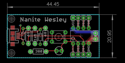
This is the continuation of a series of articles demonstrating how to Create A PCB In Everything. In this series, we take a standard reference circuit and PCB layout — a simple ATtiny85 board — and build it with different PCB design tools. Already, we’ve taken a look at the pre-history of PCB design with Protel Autotrax, we learned Fritzing is a joke for PCB design, and we’ve done a deep dive into Eagle. Each of these tutorials serves two purposes. First, it is a very quick introduction to each PCB design tool. Second, this series provides an overall comparison between different PCB design tools.
Now, finally, and after many complaints, it’s time for the tutorial everyone has been waiting for. It’s time for KiCad.
No, like the head of the Bajoran clergy
Although KiCad (pronounced ‘Kai-Cad’ like the head of the Bajoran clergy, not ‘Key-Cad’ like the thing that goes in a lock) is the new hotness when it comes to PCB design. The amazing growth of KiCad installations over the past few years is a long time coming. In development since 1992, KiCad has cemented itself as the premier Open Source PCB design suite, and since 2013 CERN has been making contributions to the project. More recently, the KiCad project has been showing off some amazing new features. These include 3D rendering of boards, interactive routing, push-and-shove, simulation, and dozens of other features that put it on a path to being on par with the top of the line EDA suites. Add in some great community contributions, and you have something really, really amazing. All of this is wrapped up in an Open Source license, free as in speech and beer. If you’re looking for the future of PCB design, Eagle is going to get very good but KiCad is almost there now while being Open Source.
The KiCad Overview
As I said in the introduction to this series of posts, this tutorial will be broken down into three main parts. The first will be how to create a part — specifically a DIP8 ATtiny85 — as a schematic symbol and how to create the schematic we need. The second part of this KiCad tutorial will assign footprints to our symbols and turn the schematic into a board you can send off to a fab house. Finally, we’ll take a look at the cool features of KiCad, such as push and shove routing and 3D rendering.
For this part of the KiCad tutorial, we will only concern ourselves with making a part for a DIP8 ATtiny85. Download KiCad and let’s get started.
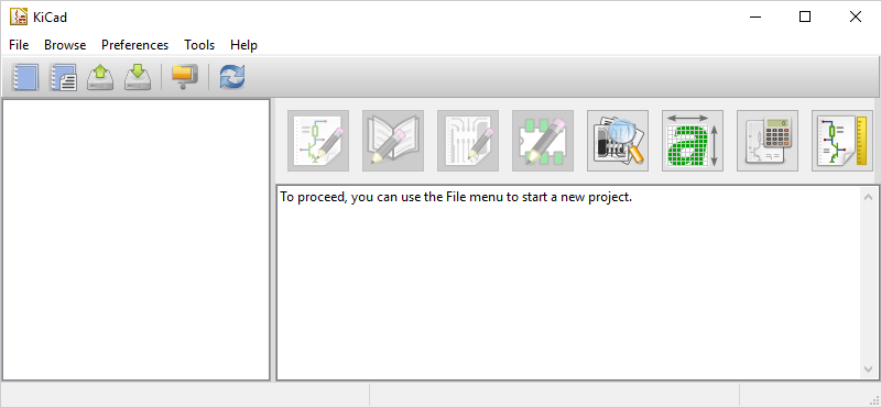
Just like Eagle – and every other PCB design tool, for that matter – there are several different editors in KiCad. They are:
![]()
Eeschema – the schematic editor
![]() The Schematic library editor – used for editing part libraries
The Schematic library editor – used for editing part libraries
![]() Pcbnew – the ‘board’ editor
Pcbnew – the ‘board’ editor
![]() The PCB footprint editor – used for editing footprints (the physical package) of parts
The PCB footprint editor – used for editing footprints (the physical package) of parts
An introduction to the terminology of PCB design might be in order. A schematic is the abstract design file, showing the electrical connections between all the components in your circuit. The schematic is not sent to the fab house.
A PCB or board describes the layout of the components, holes, pads, traces, connections, mechanical design, and silkscreen. Designing a board is the end game of all PCB design work, and it is this file that gets sent off to a fab house for manufacturing.
Before we put together a schematic and design a board, we must learn how to build our own parts. To start, install KiCad, select File -> New Project, and name it ‘Nanite’, or ‘Some Trash I’ll Never Do’
Making A Part
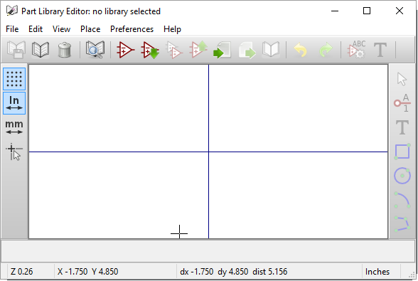
All of these tutorials demand making a part from scratch. Right now, that means making a part and footprint for a DIP8 ATtiny85. From the main KiCad window, open up the Part Library Editor, and you have a window that looks like this:
When you first open the Part Library Editor, no libraries are loaded. You would think it would be possible to simply create a new library, and design some parts, but KiCad is weird. To make your own library in KiCad, you must first select an existing library and save it as your own. Yes, it’s a bit weird and one of the many oddities of the KiCad UX, but at least it’s better than Fritzing.
 Save this library you just ‘created’, select File -> Current Library, and select the library you just saved. Now we can begin to make a part.
Click the ‘Create a new component’ opamp icon, and you’re presented with a window asking you to name your part. For small, simple, jellybean components, you won’t have to bother with anything except for the name. Name your part ATtiny85 and click okay. The name and designator of the part will be dropped into the window. Now we’re ready to add pins to our part.
Oh God Everything Is Backwards And My Mouse Doesn’t Do Anything
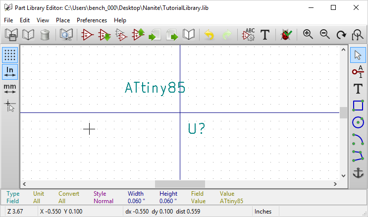
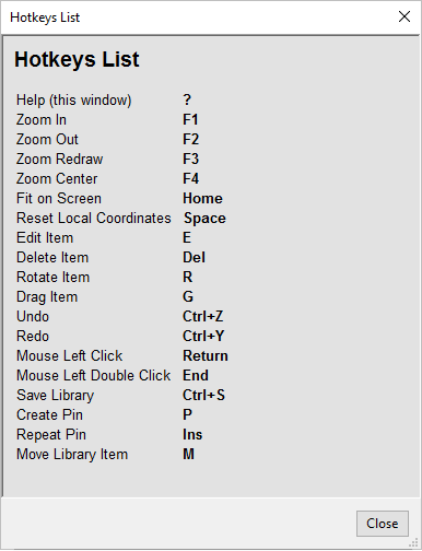 If you’re following along with this tutorial, this is the first time you’ll actually use the KiCad interface. KiCad has a reputation for being incomprehensible for the beginner. Want some proof of that? Click on the ‘ATtiny85’ label and try to move it. You would think just clicking it would do something, but that only opens up some options (bold, italic, size, justification) for the text. If the ‘ATtiny85’ and ‘U?’ overlap, clicking on both of them opens up a dialog box.
There’s a reason for this: KiCad, like almost every other PCB design tool, is based on hotkeys. This is the reason KiCad gets the reputation for not being user-friendly, but there’s a solution: just type a question mark. The list of hotkeys will pop up, and now you’ll always know what keys you need to hit to do what you want to do. To move the ‘ATtiny85’ and ‘U?’ label off to the side, hit ‘M’ while hovering the mouse over each label.
![]() Now it’s time to add pins. Click the ‘Add pins to Component’ button on the right side of the window. Next, click anywhere on the Part Library Editor window.
Now it’s time to add pins. Click the ‘Add pins to Component’ button on the right side of the window. Next, click anywhere on the Part Library Editor window.
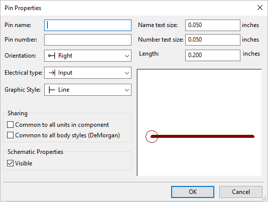
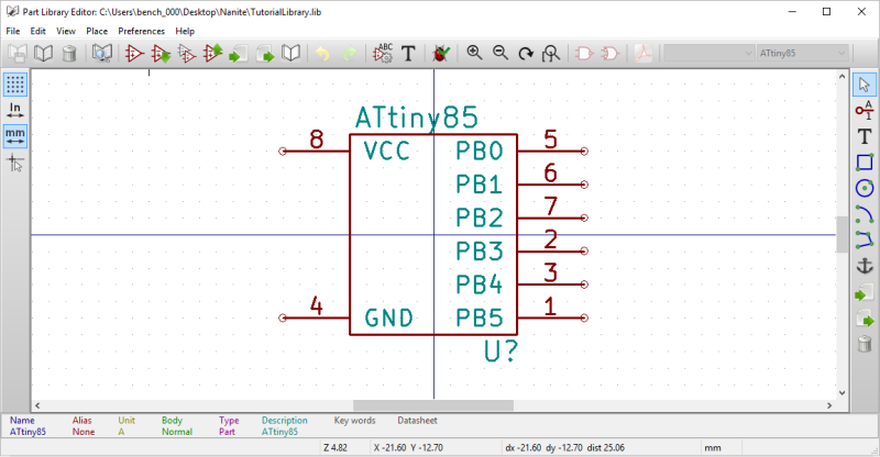
The Pin Properties window is where you assign a name, number, and graphical style to all of the pins in the schematic representation of your part. We’re doing a very simple part with power and ground on one side, and all the IO on the other side. As long as the pin names are correct, and all the pins correspond to the correct numbers on the footprint, you shouldn’t have much trouble. The only thing that might trip you up is the orientation of the pins; here, the circle at the end of each pin designates where the pin connects to a net on the schematic.
Drop eight pins down and make your part look something like what we made in the Eagle tutorial. You’ll end up with something like this:
With the pins dropped into the window and correctly labeled, all we need to do to finish the part is to draw a rectangle. Click on the ‘draw a rectangle’ icon, click once in the corner, drag, and click again to finish the rectangle. Hit File -> Save Current Library, and we’re done making the schematic symbol for this part.
From Symbol To Schematic
Now that we have a symbol for the ATtiny85 we’re going to use in this board, it’s time to make a schematic. From the main KiCad window, open up the Electronic Schematic Editor, and you’ll be presented with the following window:
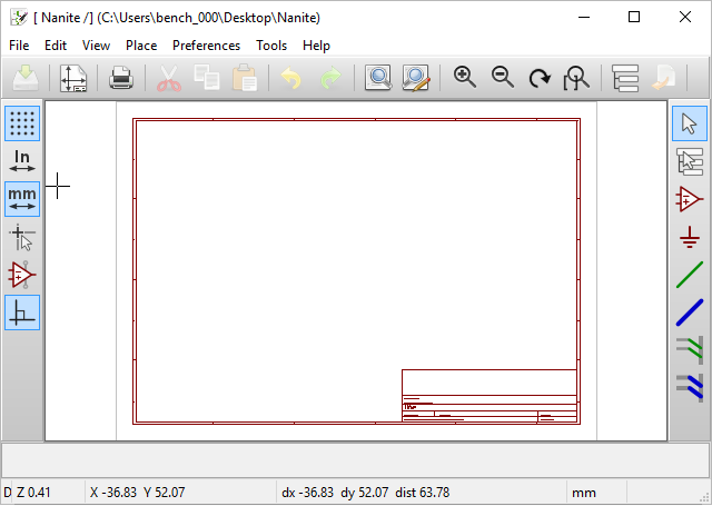
Again, the hotkeys are going to kill you. To add a component, press ‘A’. You might also want to hit ‘?’ and bring up the list of hotkeys.
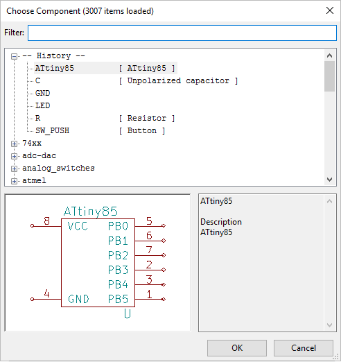
At this stage, we’re not concerned with footprints, or the physical dimensions of the components we’re eventually going to place on the board. All we want are symbols. There are hundreds of different varieties of USB connectors, but right now we don’t care. All we need to do is drop a few resistors, diodes, connectors, and other parts onto the schematic. To do that, press ‘A’, and the window below will pop up.
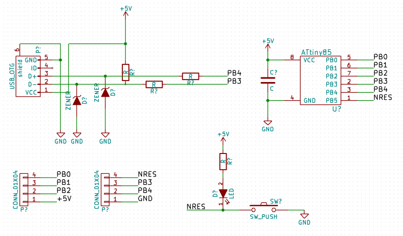
Since we’re directly copying the reference schematic from the introduction to this series, we need the following components:
- Two 1×4 connectors
- Two Zener diodes
- Four resistors
- One LED
- One USB port (OTG)
- One unpolarized cap
- One ATtiny85
- A smattering of +5V and GND symbols
For each of those components, press ‘A’ to add a part, search for the part, and drop it onto the schematic. If you’re really good, you can use the ‘P’ hotkey to add power and ground parts. When you’re done, you should have something that looks like this:
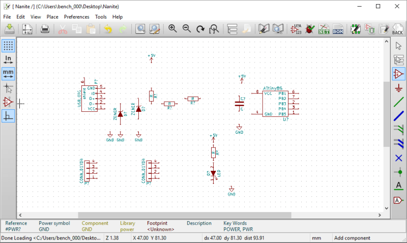
The important hotkeys to know are ‘A’ to add a part, ‘M’ to move a part, and now ‘W’ to add a wire between parts. Again, pressing ‘?’ displays a list of hotkeys. Of special interest is the ‘K’ hotkey to stop drawing a wire.
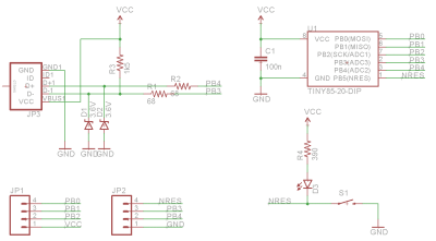
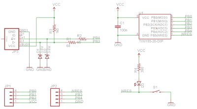 With all the wires drawn, it’s time to label these wires to connect them into ‘nets’ Check out the reference schematic to the right. The wires coming off the USB/Zener/resistor chunk of the schematic are labeled ‘PB4’ and ‘PB3’. These are nets connected to the PB4 and PB3 pins on the ATtiny, and are used for USB communications. The 1×4 headers are connected directly to every pin on the ATtiny, so we label them accordingly.
To label these wires and turn them into nets, use the ‘L’ hotkey, and select a name for each of your nets. Drop this label over the open connection on each wire to turn them into nets. When you’re done, you’ll have something that looks like this:
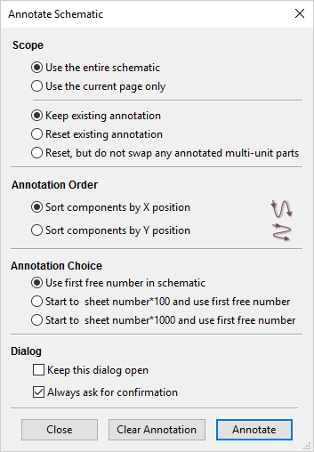 We’re almost done with the schematic. All we need to do now is add values to the relevant parts. The resistors must be labeled with the right value, the capacitor should 22nF or thereabouts, and the Zeners should have a ‘3.6’ label. It’s time for hotkeys again, this time brought to you by the letter ‘V’. Press ‘V’ over all the caps, resistors, diodes, and the LED and assign values. This takes care of the values for each part, but we still need to give each part a name. To do this, we’re going to use the ‘Annotate Schematic’ tool available in the top toolbar.
The Annotate Schematic tool automatically assigns a letter (D for diodes, L for inductors, R for resistors, Q for transistors…) to each part, along with a number. There are options to set how these numbers are assigned, but this is a very simple circuit and simply pressing the ‘annotate’ will suffice.
With that, our schematic is done. We haven’t set any footprints up for each part, and we haven’t even started on the board yet. This post is already two thousand words long, though, and Hackaday readers have the entire Internet has no attention span.
In the next part of this KiCad tutorial, we’re going to take a look at assigning footprints (the physical representation of components) to the parts in our schematic. We’re going to make a board, after which we’ll take a look at DRC, and a few of the neat tricks in KiCad including 3D rendering, turning the board into a bunch of Gerbers, and send off to a fab house.




Was thinking about giving kicad a go to move away from proteus, which is expensive and obscure, but I think I change my mind. Eagle would never run right for me and always find a way to crash and destroy any work that I’ve done with it. I think I’ll stick with obscure and just keep making my own footprints when I need to. Hotkeys for everything is just dumb.
I disagree, the hotkeys have allowed me to do layouts much faster in KiCAD as well as schematic capture. After using it for about 3 months I feel its as capable as Altium designer which is what I have been using for years. KiCAD is also 100% free and open source, so its not depended on proprietary updates that cost tons of money. Also for the most part I make 100% of my own footprints because you can’t trust the ones you find on the web, best to make them all according to MFR specs because IPC isn’t universally followed.
It shouldn’t take 3 months to learn to edit a schematic, it should be on the order of 3 hours. Making the mouse and keyboard commands more standard would go a long way to fixing that. How long does it take the average user to figure out how to select a component in order to edit it. Order seems to be all messed up too, to place a component you’d expect to pick a component first and then place it.
LOL it took me 3 minutes to learn the entire suite of applications, I’ve been using it as my main design tool for 3 months as in designing multiple full PCBs projects. I was merely stating that having used it for 3 months my evaluation is that its as good as a urber expensive professional option.
I’m glad it works for you. I found the KiCad interface to be a cluster….
I wouldn’t mind some extra buttons for commands on KiCad. That said, now that I got used to the hotkeys I can’t use Eagle anymore. I’m always trying to use the hotkeys and notice how good it is to have them.
It took me a while to have the courage to switch from Eagle to KiCad, but now I can say I don’t regret learning to use KiCad.
Though libraries in KiCad really are weird.
I want to learn kicad, but find so much too troublesome.. like the drc, I mean common.. you can’t import rules, you have to keep a template for each boardhouse. And if you decide to change fab during a project, you have to enter everything manually, thats stoneage. Also, the first thing I did when I started learning eagle was to map my own hotkeys, both on mouse and keyboard. So its not like eagle doesn’t have the feature.
I’ve been using KiCad for 10 years now, and yes, I still find the way libraries work to be weird. As for the contents of those libraries, I almost never use them. I’ve created my own, because the style and the dimensions of the included libraries were never to my liking. But for all its quirks, I can’t see myself using anything other than KiCad – it’s powerful, it’s ‘free as in speech’, and it’s available for Linux. That last is very important – I don’t really ‘do Windows’ any more, and haven’t for many years.
You are the guy I would want to make a video or PDF about kicads kinks and quirks. I cover most my needs with Eagles free version, but I have a couple of project that will need kicad. I really want to go open source, having been ‘windaows’ free the last few years. Productivity is soo much better with a REAL OS!
This is really perplexing to me. Hotkeys to speed up frequently used items makes sense, but to not ALSO have the functionality in the mouse and menus really doesn’t make sense to me. Is there a reason for this?
All commands can be accessed either via hotkeys, or mouse context Menus or just clicking the Menu / Icons.
I agree with the sentiment regarding hotkeys; with no equivalent in the GUI, for an intermittent user where you go to use the software cold after a few months of not using it, having to re-learn the hotkeys every time is a deal breaker.
Everything *does* have a GUI equivalent; either in the main menus, toolbars, or the right-click context menu. There’s nothing that’s hotkey-only.
All such tools have quirky interfaces. GIMP for example is so weird to me I can’t wrap my head around doing even basic things and give up.
The “Getting to Blinky” tutorials on YouTube really helped me get up to speed.
And yeah, after learning to really drive it, KiCAD is pretty good. The quirks and speed bumps are easy enough to minimize.
Until you get used to Hotkeys, use the context menu. Context-Click on your area of interest, example a Resistor, and you’re presented with all the available and relevant commands. If your mouse is overlapping two items (example a Wire and a Junction, or a Value and a Reference), you’re first asked to decide which one you’re interested in.
Except Brian is completely wrong here – every function is also available in a menu. If you don’t look at the right-click context menu then you miss a bunch of stuff.
Don’t brush it off that easily. As someone who moved from Proteus to KiCad recently, it took around a morning of initial frustration to enjoying it! That morning is more than offset by the library of parts I don’t have to make, money spent on a licence and risk of using outlier software.
Thanks for the well written article Brian!
Have been meaning to give KiCAD a whirl for a while now and this article pushed me to finally doing it.
“The French pronunciation is near KeeCad”
https://en.wikibooks.org/wiki/Kicad/FAQ#What_is_the_official_name_for_KiCad_EDA.3F
Well then it’s a good thing we’re reading English here.
Also, that wiki is wrong. Orthographically, it’s KiCad. No Kicad or KiCAD. Even the URL is wrong. Horrible resource.
Even Chris Gammell recognizes ‘key cad’ as being the correct pronunciation.
https://forum.kicad.info/t/how-to-pronounce-the-word-kicad/4227/15
Oh, and if my resources are so horrible, what exactly are your resources for supporting ‘kai cad’? As of now that’s just a bald assertion.
This!
Some sources here and there to back up claims would be grand :)
Here you go. It’s Chris Gammell, saying ‘Kai’ cad at 20 seconds. Yes, I’ve read the sources on what it ‘should’ be, but that doesn’t matter. The only thing that matters is the pronunciation people actually use. Since a *lot* of people have learned KiCad from Chris, ‘Kai’ is probably the most dominant pronunciation.
https://www.youtube.com/watch?v=JN_Y93RTdSo&t=20
Jesus fucking christ I should not have to defend myself to this extent concerning things that do not matter at all. At. All.
Okay Brian, calm down, check your blood pressure.
We all know how Chris pronounces it. That’s why I provided the second link that you ignored, wherein he disagrees with you. (That thread is incidentally where I got the first ‘horrible resource’, and I don’t see anyone there bitching about it. I guess they’re not as discerning as you.)
You can go with ‘probably popular’ makes right if you want, but that’s a pretty crappy argument. And if you’re going to assert incorrect things as fact and then blow up when challenged on them, you really ought to reconsider your career choices.
I’m French, like JP, the local pronounciation should be “Kick Ad”… you know what ? We don’t care, call it “Cake Add”/”Kwaek Eid” but use it, kick (Ad) the proprietary software out of the boardhouse.
I’m Swedish, pronounce it somwhere in between kee-cad and kick-ad. More towards a short kee-cad
The only opinion that matters regarding pronunciation belongs to Jean-pierre Charras.
I personally use “key” but that is partly due to language training living in Japan. ki is pronounced “key” here. And I often say both in a sentence. It’s a bit ridiculous. “Hey I want to teach an intro to KaiCad/KeyCad. Anyone interested?”
I prefer to pronounce it Kick Add
Key Cad? Kai Cad?
Screw you all, I’m gonna keep calling it Kick Ad.
Not easy to switch between pcb and schematic…
(I’ve commented on this in the past)
What do you mean? I sort of like the fact that schematic capture and PCB layout are separate applications/windows it would be nice for them to all be dockable in a single GUI for folks that don’t like them separate but with two monitors I prefer the separate application approach. That being said in the developmental roadmap they are going to have all the applications dockable to a single GUI or as tabs.
http://www.ohwr.org/projects/cern-kicad/wiki/WorkPackages
I noticed something interesting with the 4.0.4 stable Kicad on OS X Sierra. Start by opening the Kicad project manager. Then open your top-level schematic or your PCB. They open in tabs! This is a new Sierra feature but I didn’t expect it to be supported by wxWidgets. Of course you can just drag a tab out of the window and it opens in its own window.
And remember that in Kicad, when you have your schematic and your PCB open at the same time, when you click on a part in one (say the layout), it’s automatically selected in the other (the schematic).
Does your computer not have alt-tab?
Ideally you can have both windows open, one on each monitor, with net / component highlighting transferable between the schematic / PCB. Altium does this.
Thanks for the tutorial! I’d had a go with kicad before, but, predictably, found it a bit obscure.
You seem to be getting noticeably saltier with every one of these articles. I guess this is unavoidable.
No, you do not need to give values or names to the components! The only required thing to do is to associate a footprint with each one.
Sure, you don’t *need* to, but if you don’t, you run the risk of wondering what the hell it was you designed when you look at it a month later.
I commend you for at least trying out KiCad. However, I’m a bit surprised by your problems. Most problems I’ve had with KiCad originate from the reimplementation of the graphics abstraction layer in PCBNew. Instead of just reimplementing, they seem to be very open to changing hotkeys arbitrarily. But I digress …
1) Creating new libraries shouldn’t be a problem without copying another library.
You simply create a new footprint and then select File>Save Footprint In New Library. That’s it. For the next footprint, you select the library you just created as the active library and add the new footprint to this library. I’m not sure if you can do it in a much better way. I certainly don’t need to wrap my brain around it.
2) Double-clicking on an element brings up its properties. Had you ever tried to right-click on an element, you would have gotten a menu with an ample amount of operations, e.g. move, rotate, … — this is quite convenient, as this menu also lists the corresponding hotkeys for these actions.
3) Eagle and KiCad share different tool usage philosophies. In Eagle, you first select the tool, then you select the elements to use the tool on. In KiCad, you first select the element (by hovering over it with the mouse), then you select the tool. I’d say which one you like is mainly a matter of taste. I usually prefer the “tool, then element” approach. However, most software uses “element, then tool.” For example, how do you make a text bold in Word? You first select the text, then you click on “bold,” which is more akin to how KiCad handles tools. Thus, you could hardly argue that it’s fundamentally unintuitive. If Word were to work like Eagle, you’d first select “bold” and then click on the words you want to make bold.
Granted, KiCad isn’t perfect. In my opinion, usability is the biggest problem. There aren’t hotkeys for everything, so you need to use your mouse often–too often for my taste. The mouse in a CAD program should be responsible for moving things around and drawing, not for selecting options from menus all the time.
And of course, you pronounce it Key-Cad. That’s how it was intended, even if you’d name it differently if you wanted the pronunciation as an American. After all, the rest of the world also pronounces American names the way they were intended.
How easy is it to back annotate in kiCad? for example, if I wan to add a forgotten
bypass cap AFTER I have routed a bunch of traces on the board, can I simply add
the cap in the schematic and have it appear (with rats-nest wires) in the board area
like they do in Eagle? I like Eagle, I have used it for years, (despite the fact that
the schematics are somewhat ugly) and the main reason I love it is how easy it is
to do forward / back annotation. In Eagle, the schematic is never considered “done” — you
can freely edit the schematic as you route the board. Is this easy to do in Kicad?
You add the part to the schematic, reannotate to give a name/number to the part (or rename everything), select the footprint, generate the new netlist and load the new netlist on the board.
If you reannotate everything, you’ll probably have some trouble in the PCB, but adding forgotten items with new names is simple.
I find this part of KiCad not as smooth as Eagle’s, but it’s not that bad.
the idea of this control of flow I personally like, but there is a one click approach in reaches or pcbnew from tool: update PCB from schematic.
I like it too. It’s just not as smooth as Eagle.
Being able to choose the footprint independently from the schematic part is one of the things I really like about KiCad. Maybe an autogenerate netlist option could be included in the future, for most projects I wouldn’t mind having it enabled.
If you do need to reannotate everything, you can import the netlist matching the components by timestamp instead. You’ve got to be careful though, any components that you’ve actually replaced will be sensed as a new component since the timestamp on the schematic component won’t match the timestamp of the component on the board. But, it does allow you to easily update the refdes on a schematic if you’re careful about when and how you import your netlists.
That’s not back annotate, it’s re-annotate.
To back annotate, you add (for example) a filter capacitor to the PCB layout, and it turns up in the schematic.
And, as far as I know, KiCad can’t do it.
Kicad cannot back-annotate. The main use for back-annotation is to “geographically” renumber the reference designators, for the convenience of your assembly tech! However, there are a couple of Python scripts which do that, and they work well.
Kicad does not support adding a part in the layout and then back-annotating that part and its connections to the schematic. That would make one helluva mess. When adding a part, you need to do it in the schematic, then update the layout from that.
This was my point when I said :
dmalhar says:
November 17, 2016 at 10:43 am
Not easy to switch between pcb and schematic…
(I’ve commented on this in the past)
KiCad is the Blender of EDA software, powerful software but a PITA to use. It seems like the designers strived to make the process and user interface as unintuitive as possible.
I haven’t found it that hard to use, its a lot like Altium and PADS.
Do you remember how you felt the first time you used them? Thats how many KiCad users feel right now.
EVERY EDA tool is a PITA. Every last one. KiCad is no worse than any other equally powerful suite.
If you think one specific suite is “intuitive”, then it’s *only* because that’s the one you learned the quirks of and don’t recognise them as weird anymore.
Easiest “EDA” tool is ExpressPCB. It doesn’t do components on the bottom. There are absolutely no design rules. It’s expensive and doesn’t make gerbers (you have to order PCBs to get them.)
If you can draw a picture, you can use it though.
I use Altium professionally. I tinker with KiCAD but it’s interface is just really, really different.
So, you wrote an entire paragraph about the “weirdness” of KiCad, but skipped the instructions how to get around this “weirdness”, i.e. how to open an existing library and then how to open the library that you create (and the corresponding procedure of adding your library to the list).
I’m sorry if I sound too picky, but a novice will most likely be lost right after “… open up the Part Library Editor”. Or maybe my assumption that this is some kind of an introduction to KiCad for first-time users was wrong and this is just a quick overview of how the design process differs from the other PCB design packages?
Yeah this is the first thing I noticed. Instructions on getting around the weirdness would be great, I’ve used KiCad for a couple projects before and fortunately never had to play around with libraries much at all, but my next project is gonna be heavy on custom footprints so I’d like to know how.
“To make your own library in KiCad, you must first select an existing library and save it as your own.”
No, you make a new component, then you click the “Save Component In New Library” button. Which is completely straightforward.
The only thing stopping me from adopting KiCAD is the scripting interface. There seems to be some abilities using python but it does not do everything that can be done by hand. Seems like an afterthought.
Any decent professional PCB CAD tool should have a scripting interface to do batch processing and automation. This is very lacking in KiCAD
I just don’t agree that Fritzing is a joke. I find this kind of comment quite frustrating.
In terms of going from an idea, to schematic, to PCB, there is nothing quicker for a newbie. It was my entry level drug in terms of laying out PCB’s and getting stuff made by OSHPark, and it gets the job done! I agree that there are more flexible, complicated tools, but they are no where near as user friendly.
I think this is a case of auther bias.
Yes, fritizing might be a joke to you but to my 9 and 10 year old kids its workable and they like using it. please quit with the (negative) opinions on everything, just present the facts and let us decide.
Funny, for me it was the other way round. I started with eagle and was frustrated and annoyed. Then I used KiCad the first time and the concept behind was pretty straight forward, ok except the part with the footprints, but after some googling I came along with it and I like it. And after working with HyperWorks you will never ever complain about any userinterface-concept again. Compared to this meshing with Salome is easy cheesy……and far more reliable.
“With that, our schematic is done. We haven’t set any footprints up for each part, and we haven’t even started on the board yet. This post is already two thousand words long, though, and Hackaday readers have the entire Internet has no attention span.”
You probably could have fit a lot more explanation into that same word count if you turned down the snark a little bit… no.. a lot and just got down to business already. OK, you like Eagle. We get it. Maybe it would have worked out better if each article was written by someone who actually prefers to use the suite they are describing? Or maybe somebody who has never used any suite at all could write about the process of learning them from scratch?
Anyway.. you even went into an explanation of what schematics and layouts are. Does anyone who would chose to read this series not already know that? And if so shouldn’t it have been explained on the first post rather than when on the third of fourth or whatever this is? Hey.. by the way… since we have been talking about how to make these things for a few months how about we take a moment to explain what they are now….?
So.. umm.. yah… 2000 words. All right then.
Agreed. In fact, it would be great to have “Revisited: Creating a PCB in X – Written by a Fan”
A series of articles that run tandem to these, written by people who are biased towards the target applications. If all the articles are biased, then the entire series itself is not bias; understand my logic?
Eitherway, I appreciate the effort you have put in Brian, its not small effort writing all of these article. However I wish they were a little more informative, with less opinion.
DesignSpark PCB. Try it!
Your USB lines are mismatched #amauterhour
Also its easy to download a user supplies library rather than creating one from scratch. You could probably find the chip your using.
I did the tutorial but could not find the push button in the library of components. Did I miss installing something?
This was a _frustrating_ tutorial because of missing items. You must manually add the switch library: Preferences->Component Libraries->Add->Choose switches.lib.
You should not need to do that unless something weird has happened. Make sure you are using the latest stable version and not nightly build.
Just installed the latest stable version today, and I had to do this. But in a way it’s good having to figure something out. Adds to the learning experience, I guess. :-D
it is TIME, to start learning KiCAD.
Just started learning KiCad and following this tutorial. Strikes me (a total newbie) it needs some up dating or at least some improvement on detail. Right off the start I can’t find the “Part Library Editor”. Even in the list of editors there is no editor for parts – Symbols: yes, Parts: no. I suspect the KiCad folks have changed things a bit which would explain some of the differences but …
Which version of KiCad was used to make this article?
Yeah, needs a refresh. This was made with KiCad 4.0, now we’re on 5.0.
I just wanted to leave a quick note to say that I am very grateful for this tutorial. I keep coming back to this set of articles because I don’t use the app that frequently and I keep forgetting the basics of the workflow. This tutorial is always the perfect refresher, so many thanks for writing it!