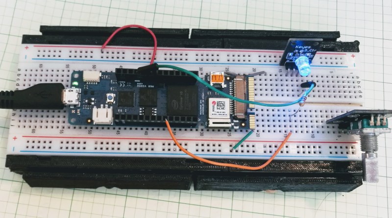
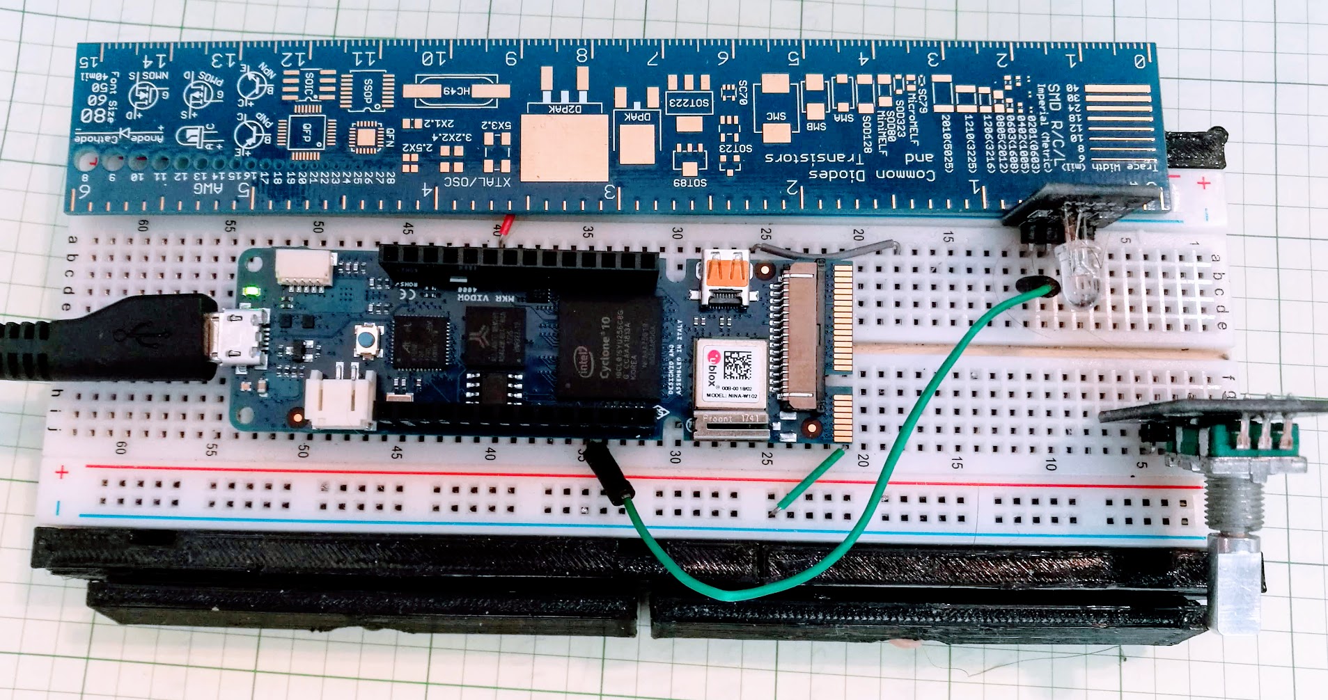
Hackaday brought you a first look the Arduino MKR Vidor 4000 when it announced. Arduino sent over one of the first boards so now we finally have our hands on one! It’s early and the documentation is still a bit sparse, but we did get it up and running to take the board through some hello world exercises. This article will go over what we’ve been able to figure out about the FPGA system so far to help get you up and running with the new hardware.
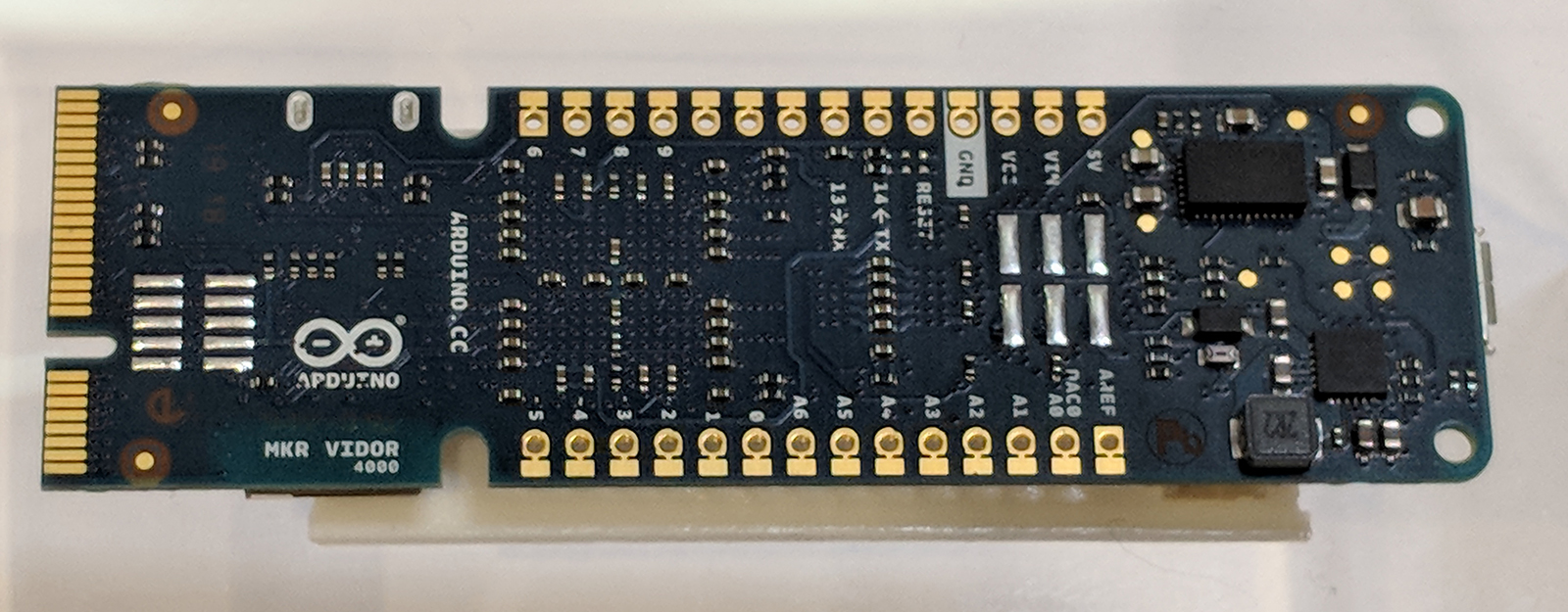
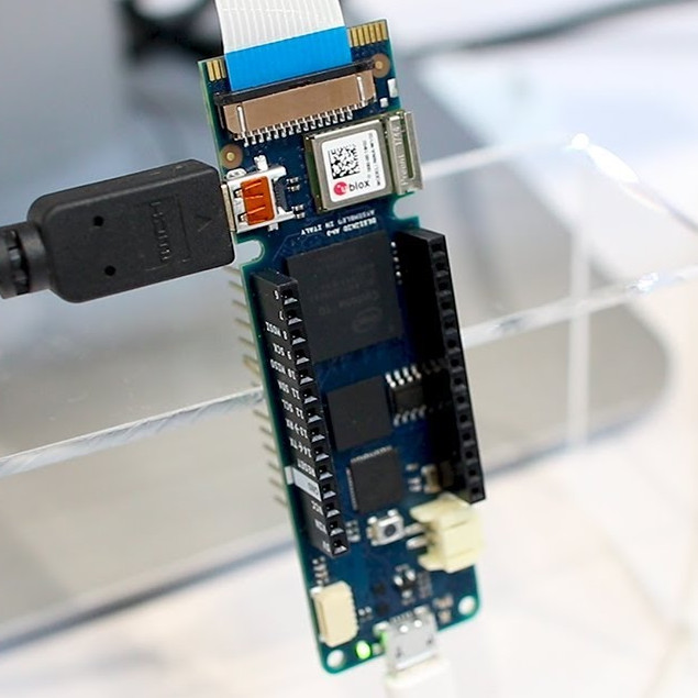
Just to refresh your memory, here’s what is on the Vidor board:
- 8 MB SRAM
- A 2 MB QSPI Flash chip — 1 MB allocated for user applications
- A Micro HDMI connector
- An MIPI camera connector
- Wi-Fi and BLE powered by a U-BLOX NINA W10 Series device
- MKR interface on which all pins are driven both by SAMD21 (32-bit ARM CPU) and FPGA
- Mini PCI Express connector with up to 25 user programmable pins
- The FPGA (an Intel/Altera Cyclone 10CL016) contains 16K Logic Elements, 504 KB of embedded RAM, and 56 18×18 bit HW multipliers
Sounds good. You can get more gory technical details over at Arduino and there’s even a schematic (.zip).
Documentation
Documentation is — so far — very hard to come by but the team is working to change that by the day. Here are the resources we’ve used so far (in addition to the schematic):
- A getting started guide
- A GitHub site with three repositories: An example for general I/O in the FPGA, an example for video, and a stripped down example that loads an unknown — possibly default — bitstream
- A very generic document about FPGA coding
- The forum for the MKR 4000
In addition, Arduino just released an example FPGA project for Quartus. I’ll explain what that means in a bit.
Get Up and Running with the Arduino Desktop IDE
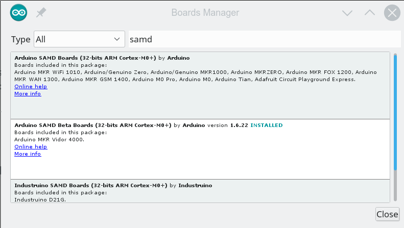
Despite the getting started guide, it doesn’t appear the libraries are usable from the cloud-based IDE, so we followed the instructions to load the beta board support for the MKR 4000 into our desktop IDE. Be aware that the instructions show the “normal” SAMD board package, but you actually want the beta which says it is for the MKR 4000. If you search for SAMD in the Boards Manager dialog, you’ll find it (see the second entry in the image below).
The libraries we grabbed as ZIP files from GitHub and used the install library from ZIP file option with no problems.
What’s the Code Look Like?
The most interesting part of this board is of course the inclusion of the FPGA which left us wondering what the code for the device would look like. Browsing the code, we were a bit dismayed at the lack of comments in all but the JTAG code. We decided to focus first on the VidorPeripherals repository and dug into the header file for some clues on how everything works.
Looking at VidorPeripherals.h, you can see that there’s a few interesting I/O devices include SPI, I2C, UART, reading a quadrature encoder, and NeoPixel. There’s also a few headers that don’t exist (and presumably won’t get the define to turn them on) so don’t get too excited by some of the header file names until you make sure they are really there.
Then we decided to try the example test code. The library provides a global FPGA object that you need to set up:
// Let's start by initializing the FPGA
if (!FPGA.begin()) {
    Serial.println("Initialization failed!");
    while (1) {}
}

// Let's discover which version we are running
int version = FPGA.version();
Serial.print("Vidor bitstream version: ");
Serial.println(version, HEX);

// Let's also ask which IPs are included in this bitstream
FPGA.printConfig();
The output of this bit of code looks like this:
Vidor bitstream version: 1020107
number of devices 9
1 01000000 MB_DEV_SF
1 02000000 MB_DEV_GPIO
4 04000000 MB_DEV_I2C
6 05000000 MB_DEV_SPI
8 06000000 MB_DEV_UART
1 08000000 MB_DEV_SDRAM
4 09000000 MB_DEV_NP
11 0A000000 MB_DEV_ENC
0 0B000000 MB_DEV_REG
In many cases, the devices provided by the FPGA are pretty transparent. For example, here’s another snip from the example code:
// Ok, so we know now that the FPGA contains the extended GPIO IP
// The GPIO pins controlled by the FPGA start from 100
// Please refer to the online documentation for the actual pin assignment
// Let's configure pin A0 to be an output, controlled by the FPGA
FPGA.pinMode(33, OUTPUT);
FPGA.digitalWrite(33, HIGH);

// The same pin can be read by the SAMD processor :)
pinMode(A0, INPUT);
Serial.print("Pin A0 is ");
Serial.println(digitalRead(A0) == LOW ? "LOW" : "HIGH");

FPGA.digitalWrite(33, LOW);
Serial.print("Pin A0 is ");
Serial.println(digitalRead(A0) == LOW ? "LOW" : "HIGH");
That’s easy enough, and it is nice that the pins are usable from the CPU and FPGA. We couldn’t find the documentation mapping the pins, but we assume it is coming.
Using, say, an extra serial interface is easy, too:
SerialFPGA1.begin(115200);
while (!SerialFPGA1);
SerialFPGA1.println("test");
Bitstream
So where’s the FPGA code? As far as you can tell, this is just a new Arduino with a lot of extra devices that connect through this mysterious FPGA object. The trick is that the FPGA code is in the library. To see how it works, let’s talk a little about how an FPGA operates.
When you write a program in C, that’s not really what the computer looks at, right? The compiler converts it into a bunch of numbers that tell the CPU to do things. An FPGA is both the same and different from that. You write your program — usually in a hardware design language like Verilog or VHDL. You compile it to numbers, but those numbers don’t get executed like a CPU does.
The best analogy I’ve been able to think of is that an FPGA is like one of those old Radio Shack 100-in-1 electronic kits. There are a bunch of parts on a board and some way to connect them with wires. Put the wires one way and you have a radio. Put them another way and you have a burglar alarm. Rewire it again and you have a metal detector. The numbers correspond to wires. They make connections and configure options in the FPGA’s circuitry. Unless you’ve built a CPU, there’s nothing in there examining and acting on the numbers like there would be with a CPU.
The numbers that come out of an FPGA tool is usually called a bitstream. Someone has to send that bitstream to an FPGA like the Cyclone onboard the Arduino every time it powers up. That someone is usually a memory device on the board, although the CPU can do it, too.
So that leads to two questions: Where is the bitstream? How does it get to the FPGA?
The answer to the first question is easy. If you look on Github, you’ll see in the library there is a file called VidorBase.cpp. It has the following lines:
__attribute__ ((used, section(".fpga_bitstream")))
const unsigned char bitstream[] = {
    #include "app.ttf"
};
What this means if there is an array called bitstream that the linker will put it in a specially marked section of memory. That array gets initialized with app.ttf which is just an ASCII file full of numbers. Despite the name, it is not a TrueType font. What do the numbers mean? Hard to say, although, in theory, you could reverse engineer it just like you can disassemble binary code for a CPU. However, it is the configuration required to make all the library calls we just talked about work.
The second question about how it gets to the FPGA configuration is a bit of a mystery. As far as we can tell, the bootloader understands that data in that section should get copied over to the FPGA configuration memory and does the copying for you. It isn’t clear if there’s a copy in the main flash and a copy in the configuration flash but it seems to work transparently in any event.
There’s a checksum defined in the code but we changed it and everything still worked. Presumably, at some point, the IDE or the bootloader will complain if you have the wrong checksum, but that doesn’t appear to be the case now.
By the way, according to the Arduino forum, there are actually two bitstreams. One that loads on power-up that you would rarely (if ever) change. Then there is another that is the one included with the library. You can double-click the reset button to enter bootloader mode and we suspect that leaves the FPGA initialized with the first bitstream, but we don’t know that for sure. In bootloader mode, though, the red LED onboard has a breathing effect so you can tell the double click works.
What about my FPGA Code?
 This isn’t great news if you were hoping for an easy Arduino-like way to do your own FPGA development in Verilog or VHDL. Intel will give you a copy of Quartus Prime which will generate bitstreams all day for you. We think — but we aren’t sure — that the ASCII format is just a raw conversion from binary of the bitstream files.
Very recently, Arduino provided a Quartus project that would create a bitstream. This provides a few key pieces of the puzzle, like the constraint file that lets the FPGA compiler find the different parts on the board.
However, even with that project, you still have some reverse engineering to do if you want to get started. Why? Here’s what Arduino says about loading your own FPGA code (we added the emphasis):
Quartus will produce a set of files under the output_files directory in the project folder. In order to incorporate the FPGA in the Arduino code you need to create a library and preprocess the ttf file generated by Quartus so that it contains the appropriate headers required by the software infrastructure. Details of this process will be disclosed as soon as the flow is stable.
Programming the FPGA is possible in various ways:
- Flashing the image along with Arduino code creating a library which incorporates the ttf file
- Programming the image in RAM through USB Blaster (this requires mounting the FPGA JTAG header). this can be done safely only when SAM D21 is in bootloader mode as in other conditions it may access JTAG and cause a contention
- Programming the image in RAM through the emulated USB Blaster via SAM D21 (this component is pending release)
In addition, the repository itself says that some key pieces are missing until they can work out licensing or clean up the code. So this gets us closer, but you’d still need to reverse engineer the header from the examples and/or figure out how to force the processor off the JTAG bus. The good news is it sounds like this information is coming, it just isn’t here yet.
Of course, you are going to need to understand a lot more to do anything significant. We know the FPGA is set in the AS configuration mode. We also asked Arduino about the clock architecture of the board and they told us:
[The CPU] has its own clock which is used to generate a 48 MHz reference clock that is fed to the FPGA (and that can be removed at any time to “freeze” fpga). In addition to this reference clock, [the] FPGA has an internal RC oscillator which can’t be used as [a] precise timing reference for tolerance issues but can be used in case you don’t want [the CPU] to produce the reference clock.
Of course, the FPGA has a number of PLLs onboard that can take any valid clock and produce other frequencies. For example, in the vision application, Arduino demonstrated, the 48 MHz clock is converted into 24 MHz, 60 MHz, 100 MHz, and 120 MHz clocks by PLLs.
Mix and Match?
 One thing that is disappointing is that — at least for now — you won’t be able to mix and match different FPGA libraries. There is exactly one bitstream and you can’t just jam them together. Although FPGAs can often be partially configured, that’s a difficult technique. But we were a little surprised that the IDE didn’t understand how to take libraries with, for example, EDIF design files for IP that would all get compiled together. That way I could pick the Arduino UART and mix it with the Hackaday PWM output module along with my own Verilog or VHDL.
The way things are structured now you will have one bitstream that is precompiled by another tool (probably Quartus for the foreseeable future). It will match up with a particular C++ library. And that’s it. Doesn’t matter how much of the FPGA is left over or how much of it you really use, you will use it all for the one library.
Of course, you can load another library but it is going to replace the first one. So you only get one set of functions at a time and someone else gets to decide what’s in that set. If you roll your own, you are going to have to roll your own all the way.
What’s Next?
It is still early for the Arduino Vidor. We are hopeful we’ll get the tools and procedures necessary to drop our own FPGA configurations in. It would be great, too, if the stock libraries were available in source format including the Verilog HDL. The recent GitHub release shows quite a bit, although it isn’t all of the examples, it is probably enough if we get the rest of the information.
As for a more intuitive interface, we don’t know if that’s in the cards or not. We don’t see much evidence of it, although posts on the Arduino forum indicate they will eventually supply an “IP Assembler” that will let you compose different modules into one bitstream. We don’t know if that will only work with “official” modules or not. However, we know the Arduino community is very resourceful so if we don’t get a good ecosystem it will not surprise us if someone else makes it happen. Eventually.
For now, we will continue to play with the existing bitstreams that become available. There are some neat new features on the CPU, too. For example, you can map two of the unused serial modules. There’s a hardware-based cooperative multitasking capability. As more details on the FPGA emerge, we’ll keep you posted and if you learn something, be sure to leave word in the comments so everyone can benefit.


Nice, now all I need to find is a router with a mini-PCI express connector.
There are plenty of “DIY” OpenWRT router boards available with MPCIE. We throw a couple wifi cards in them, mostly. Some have high-end PoE available too. A few options from Compex I’m familiar with, and probably a few from PC Engines, aside from the generic Chineseium available on AliExpress.
Unfortunately, that line of Cyclone 10 does not support PCIe. Just as a heads up to anyone who wanted a cheap PCIe FPGA dev board.
Source: https://www.intel.com/content/www/us/en/products/programmable/fpga/cyclone-10.html
Do you have any more specific locations to the information you refer to? While there may not be a dedicated set of pins for PCIe, you should be able to use either an IP block or else attempt to write one yourself. I don’t think this is a case where an M2 connector was chosen for convenience (like the Electric Imp and the RPI Compute module did with their connectors).
There are no transcievers on the 10LP family. Without those, you can’t even emulate a PCIe connection.
Do you have a more specific source for this? While there may not be a set of dedicated PCIe pins, the beauty of FPGA’s is that they are whatever you program them to be (voltage tolerances and form-factor willing). You should be able to download/buy/write an IP block that allows you to create a PCIe interface on the FPGA.
I don’t think this is the case of “convenient connectors” like we saw with the Electric Imp and Raspi Compute modules.
Check 10LP family datasheet. PCIe operates at 2.5Gbps or higher yet the fastest IO standard supported by the device comes at around 800Mbps. The only thing you can use that PCIe connector for is SIM card, USB or SM bus communication.
PCIe 1.0 transfers data at a rate of 2.5 gigabit per lane per second. With PCIe 3.0 that number has shot up to 8 gigabits per lane per second.
Unless you somehow magically overclock your FPGA to 2.5 Ghz or 8Ghz you’re going to have to rely on special multi gigabit transceivers which will set you back $300 at minimum per FPGA.
Yes, but I think you can get a couple transceivers for cheaper than $300. For example, Spartan 6 LXT series starting at $58 on digikey. I haven’t done any PCIe FPGA work, but I just remembered they were available from a project I worked on that used Spartan 6 series.
Artix 7 seems a bit cheaper. I think with today’s cheap PCB fabs and FPGAs being available at significant discounts on Aliexpress, it should be possible to put together a PCIe toy project for under $100.
Austin, while what you say is true of simple low-speed digital buses, FPGAs require analog transceivers (and often hard-IP blocks) to interface with basically any high-speed serial interfaces, including PCI Express, SDI video, Ethernet, Fibre Channel, USB, and many others. Instead of exuding over the beauty of FPGAs with annoying confidence, perhaps you should sit down and actually develop a practical project on one first?
Nice stuff!. Just like the Arduino Zero at launch time (had no information available and also few community support); It will get better over time, when people like Sparkfun and Adafruit gets their hands on writing examples for it. Waiting for it (unless you guys want to send me this board, case in which I may help do some code hahaah)
Adafruit and sparkfun are now more likely to design and release their own boards than do the groundwork on a new arduino product. Arduino 101 was undocumented and poorly supported with basic libs at launch, as a result it didn’t make it. I hope that this fairs better but arduino need to invest in seeding the community with libs, docs, videos and examples.
Arduino 101 tanked because Intel has half-assed all their maker products and then killed them when they weren’t successful instead of investing the effort to fix the obvious complaints people had.
I don’t think it was even possible to get wire libruary for i2c working reliably on the 101’s architecture. at least at the time I was attempting to intergrate my shield design to support it. Arduino jumped into bed with intel and allowed their brand be associated with a half hearted effort. hopefully they both learned from the experience and that the MKR 4000 avoids these problems.
Original Arduino was the only game in town when the original board came out. but there’s pleanty of low cost-log gate count FPGA boards out there.
As with most of the Arduino family lol.
Tastes like burning.
I’m holding out for the inevitable (and massively better) Icestorm-based board.
Letting me only load one of a set of manufacturer-provided images for the FPGA? That’s just not going to fly. With something based on Icestorm, I can load whatever design I want. I’m convinced that given an FPGA board that’s capable of fun things with video (but is limited to a set of cookie-cutter designs) and a board that lets me have fill reign over a less capable FPGA, the one where I can play around wins hands down once the hype wears off.
Just stick down an ICE40 with an Atmega and have the bootloader load up the FPGA’s bitstream either from internal flash (if there’s enough room on the chosen micro) or from an spi flash. There’ll be some fun user-experience problems to solve, but it’s all perfectly doable. (https://store.steampowered.com/app/576030/MHRD/ exists, after all (with linux support!))
I’m tempted now to just go off and make a platformio module or something that can compile C code for the Atmega and verilog for the FPGA, then link and upload. Ironically, the icestorm tools themselves are the ones probably more than mature enough. The only part I might have trouble with is designing a board around the ICE40 that obeys design rules and won’t be complete dogshit at higher speeds. (because somebody’s going to want to push the limit) Even that I could probably stumble through and get half-decent.
I might even be able to make-do if I make something that piggybacks on my existing HX8K dev board…..
Your wish has been granted, for the exact same $50 as the Vidor even: behold Alchitry’s new “Copper” board, based on an IceStorm-supported ICE40: https://www.kickstarter.com/projects/alchitry/alchitry-digital-design-simplified
Why is IceStorm such a requirement for you? Quartus is available for free, runs on Linux, and can absolutely build any FPGA image you want.
The toolchain for IceStorm has a number of advantages:
1) open source, allowing for porting to a variety of platforms
2) lightweight development environment, requiring only a handful of command-line tools (how many dependencies do you think quartus’ GUI has? How much do you want to bet it eventually has a hard dependency on systemd?)
3) open source, allowing for better integration of the tools into a workflow or to strip out unnecessary functionality.
I need to go run some benchmarks, because I’m now wondering just how lightweight the tools are.
At one point I was trying to put together an ESP8266 image with a copy of micropython and an access point/webserver that hosted a webpage-based terminal to develop it. (and maybe even some documentation!) This would have meant I could hand students one and they wouldn’t have required anything more to start playing with them.
If the Icestorm tools are light enough, then it might be possible/cost effective to integrate the FPGA with the guts of a cheap openWRT router that can provide a minimalistic development environment
How does IP -in particular the P for property- line up with OpenSource?
The FPGA IP world is not so well reputed for openess… an I even haven’t used the word “toolchain” yet.
Exactly the same as it does for software. There are tons of open-source IP cores out there, and piles of closed ones too.
There are lots of open source IP cores (opencores.org), but generally you don’t get the corresponding code for ones that come with the FPGA development environment or commercial products.
Not a word about the on-board ESP32 ?? What happened to this blog ?! :)
As announced here (in the comments, not in TFA) by the Arduino people last May, the schematics confirm that every pad of the NINA-W102 wireless module is connected to the FPGA, except for 6 of them which are still accessible via the PCIe connector (4 x ADC/GPIO + RMII management bus).
It should be possible to fetch your own firmware, compiled with Arduino IDE or ESP-IDF, for its ESP32, so a full schematic of the module would certainly be helpful for that, once published.
Well, the wireless module is mentioned right up in the first bullet list, but the point to this post was how do we get to the FPGA not how to program the onboard WiFi.
Al, thanks for this hands-on (your blog posts are totally respected and appreciated in general), that was a litle joke, and admittedly off-topic, just some additionnal information found in this board’s schematics for those interested, or simply unaware of an “ESP32-inside” wireless module. Cheers!
Well, fair point that the module is effectively an ESP32 so I’m glad you pointed that out. I’m fixated on actually putting my own Verilog in the FPGA ;)
Yes, this was very clear in your article, and we’re all in it with you :) We’re glad you shared your investigation on the actual situation with what’s been released for now, asked Arduino how it is supposed to work, and clearly some pieces are still missing, but I commend their honest communication on the subject thus far.
Probably to address a larger audience, the initial idea looks like ready-made bitstreams (virtual “shields”!) of which you can either be a user picking them, or a developper sharing them (like the Arduino libraries) and many HaD readers won’t be so pleased with a “gui-based closed-source in the cloud” FPGA toolchain that should be proposed for it…
As a reminder, here is what on of the engineers in charge and answering questions on the dedicated Arduino forum (the “Dario” that the “Brian” interviewed at Maker Fair) told us in previous comments here, following May’s announcement/presentation on Hackaday :
“As I already wrote somewhere else, reverse engineering a fpga compilation tool is not easy and works only for small, simple devices. Quartus is a very good tool but again we’re not going to ask users to install it. The compilation will happen in the cloud so you will be able to produce the fpga image even with a Chromebook or eventually a smartphone.
The blockly based GUI we’ll be releasing is much simpler than the ones in the dev tools from fpga vendors as we are trying to make it really easy to assemble systems, taking care of all the complexity behind it.”
Can the bitstream just be programmed into the config flash? After looking at the schematic I thought so but then reading this makes me think otherwise?
OT: Where do I buy that ruler?
Mine is a giveaway from Mouser. But it looks the same as https://www.adafruit.com/product/1554 except for the branding on the front. And to give equal time, I have a lovely red one that is larger from DigiKey. https://www.digikey.com/product-detail/en/digi-key-electronics/PCB-RULER-12INCH/PCB-RULER-ND/5767550
maybe you can also find the parts at this
https://www.jotrin.com/product/
Quote: “The FPGA (an Intel/Altera Cyclone 10CL016) contains 16K Logic Elements, 504 KB of embedded RAM …”
There is no such thing as “KB”
The multipliers are –
Lower case “k”: k = 10^3 or 1000 and is a decimal SI standard.
Uppercase “K” and lower case “i”: Ki = 2^10 or 1024 and is a binary unit that is not an SI standard.
The units are –
Lower case “bit” – bits, Lower case “b” is commonly used for bits but is not any standard at all
Uppercase “B” – Bytes (8-bits and not any other word length)
So the correct expressions are –
kB – 1000 Bytes
KiB – 1024 Bytes
kbit – 1000 bits
Kibit – 1024 bits
The FPGA is 504 Kibit (Binary kilo bits) of
embedded RAMBlock RAM (BRAM) arranged as 56 blocks of 1024 x 9 bits.To be fare even the data sheet gets it wrong by expressing this as “Kb” instead of Kibit.
The FPGA is 504 Kibit (Binary kilo bits) of
embedded RAMBlock RAM (BRAM) arranged as 56 blocks of 1024 x 9 bits.To be fare even the data sheet gets it wrong by expressing this as “Kb” instead of Kibit.
While that “obnoxious pedant” hat is on: to be fare some sort of means of transportation would have to be involved…
You are right it is bits. I will admit I started with a copy/paste of the Arduino catalog page (https://store.arduino.cc/usa/arduino-vidor-4000 2nd paragraph under Overview) because I didn’t want to get anything wrong. You’ll note they have it the same way. And in my head I did read it as bits ;-)
I don’t get where this is supposed to fit into the market.
They use a FPGA which is big enough for quite complex tasks that process a fair amount of information and yet there is no real high data rate inputs except for a camera and no high data rate output except for HDMI.
If it were for education then it should promote learning HDL but the inclusion of SDRAM instead of SRAM is more about plugging HDL modules together rather than writing HDL. For education there would be a lot more variation of input and output devices and yet this has nothing, no DAC no ADC, no other IO except for digital IO a camera and HDMI.
It would be great for image processing but that is not a beginners thing and Arduino has been about beginners.
The breakout system isn’t flexible enough to use any variety of modules together so any shield would have a dedicated purpose.
It could have some uses like navigation and collision avoidance for a quadcopter or something like that but the silicon is too small for any serious neural networks so your left with algorithms which would be better dome with a faster micro-controller that is cheaper and uses less power.
Perhaps gesture input to but these aren’t “beginners” things.
The ARM CPU on the board has 7 ADC inputs and 1 DAC output, and communication between the CPU and FPGA is allegedly “seamless”, so presumably the ARM would act as an intermediary. Would that be fast enough for some FPGA applications? Probably not. But it’d probably be fast enough for some applications.
I’ve yet to see how this FPGA business is more than just another gimmicky piece of hardware that’ll be completely forgotten in a year from now.
LOL
FPGA and it’s predecessors, Gate Array Logic GAL, Programmable Array Logic PAL, Complex Programmable Logic Device CPLD, have been evolving for a very long time.
Modern FPGA can now even load per-defined blocks from Serial RAM on the fly. The next evolution will be an ability for the FPGA to design other blocks on the fly without them being predefined. This will open a new pathway for neural networks.
They definitely have some unique abilities especially for parallel processing.
They also definitely have some disadvantages like cost and high power consumption.
So they’re certainly not a silver bullet technology but there are many tasks where FPGA is the obvious and only real solution.
FPGA manufacturers has watched the success of other platforms like the Arduino.
There’s nothing spectacular about the 8-bit ATmega series. The success of Arduino has been the simple IDE and the community of open source code contributions.
FPGA has transitionally been expensive walled garden IDEs and closed source IP.
Now FPGA manufacturers are trying to get that community support behind their products.
So FPGA will be around for a long time however this particular Arduino/FPGA board really misses the mark of what beginner level and open source community wants and needs, in my opinion.
Perhaps we will see another board that is better targeted in the future.
FPGA’s are surely amazing technology. I just don’t see how they can be programmed/used by the arduino crowd; typically artists and those with little to no knowledge of Electronics and programming (let alone programming hardware).
I doubt it’ll go much farther than using arduino code to download pre-made bitstreams onto the FPGA that facilitate pre-determined designs i.e. peripherals, computer vision e.t.c. VHDL and Verilog are definitely a no go. I also doubt that Arduino will put any serious effort into developing some simple HDL language to be used by novices to hardware design.
I’m having doubts that FPGAs and their “programming” languages can be made easily accessible in the same way as microcontrollers have by the Arduino platform. For me, a fairly advanced tinkerer with a bunch of experience but no engineering background, trying to get into the topic still feels very difficult, even with the explanations on the Arduino website… feels almost like trying to “get” quantum computers, or something… still, it’s nice they’re trying. Perhaps I’ll figure it out once there’s simple examples I can simply flash onto the thing and try to “learn by doing”.
Perhaps try this: https://hackaday.io/list/160076-fpga-tutorials
I always tell people it is like riding a bike or tying a necktie. It seems really hard until you can do it and then it doesn’t seem all that hard. Now some of the things you want to do with an FPGA are difficult, just like jumping a bike over 3 school bus bodies via 6 flaming hoops is hard even if you know how to ride a bike.
In February, at FOSDEM, we got a talk about ‘FPGA for kids’ : https://fosdem.org/2018/schedule/event/cad_os_fpga/
I just don’t get what it’s for. What’s the niche supposed to be?
It’s not a tool for learning about real FPGA development skills, unless you can write your own VHDL/Verilog and synthesise it onto the FPGA.
I am guessing they are not very interested in YOU writing VHDL/Verilog. They want to provide you with modules that let you customize your board. This is a common way a lot of commercial users use FPGAs. Buy up a bunch of IP blocks and string them together and make a custom chip — especially CPUs — with just the right mix of I/O for your applications. This is more common than you’d think where an “FPGA user” is really just assembling pieces and the “mixed design” tools from the vendors reflect this.
So I can see some future web tool where you say “Hmmm I would like 3 PWM outputs on these pins and 2 extra serial ports on these pins and a timer with a 4 MHz clock on this interrupt.” And you download a bitstream and library that you add to your IDE project and that’s it.
But I’m sure some of us are going to be hitting the FPGA and providing alternatives.
All this is just my prediction, of course.
Like Al and others, I hope that eventually we will “own” the whole chain for this, but the web tool is not a prediction, it was announced by their engineer (see my previous comment). When he talks about the “blockly based GUI”, we can easily think that we will be able to select functionnality blocks (like you said PWM, HDMI, etc…) and link them graphically, with a tool probaly close to a simplified PSoC Designer.
Now if you look at the origin of Arduino, the ecosystem was envisionned by “artists” (design school students/teachers) as a solution for simple electronics related to “creative” works, a bit like a customizable DMX without the need for expensive theater specialized boxes and desk : support for software controlled relays, lightning and interaction (switchs, sensors…), actually a “real world” extension for their favorite tool, Processing (from which the Arduino inherited it’s GUI to date, like the “Play” and “Pause” buttons).
First, it was a good occasion to get rid of the (probably old and grumpy) geek programming copy-protected PICs and swallowing half the budget for its black magic :) And it proved to be a good starting point then revenues for Arduino’s business. In this heavily public-funded domain, it is easier to justify expenses in high-margin hardware when it is branded and recognizable as an educational tool. Those people are generally good at spending others’ money with minimal accountability or real-world cost concerns, and evangelists for the educational market too (with the usual “taking it from the narrow-minded technicians and bringing it to the masses” self-justication) hence they probably still are one of the primary targets here.
This niche hasn’t really changed, now many “electronic artists” are just some glorified institutional VJs that worship motion tracking, augmented reality, real-time effects and video interactions, so we had OpenCV based projects all over the (arty) place for years, not always looking that great with poorly assembled, non-optimized libraries on a Rapsberry Pi…
But now they fantasize on the new trendy “black magic” : FPGAs, and I think the software for this board will try to provide them with real-time video/audio/sensor processing without the need to tinker with the (dirty and confusing) low-level stuff, like they are used to with the libraries.
Wait, Arduino can do software controlled lightning?!? Holy shit, I have to look into this right now…!
Yes. Once and only once.
I just noticed another clarifying comment posted here some weeks ago, still by Dario Pennisi and confirming this view (RTL means “Register Transfer Level” which is related to hardware description languages like VHDL and Verilog) :
“… the board is aimed primarily at existing Arduino users. Our idea is to prevent the need for RTL coding by providing lots of up blocks. The idea we’re providing allows you to just drank and drop blocks into your system on chip without any need for RTL knowledge. Basically the concept is that this board provides you the possibility to tailor it to any application, removing the limitations of the peripherals you have in the microcontroller.
Of course we’ll be delighted to see people contribute and write RTL ip blocks and I am sure it will come but again I am sure that most people will use up blocks as they today do with software libraries.”
More of the same, in the first Hackaday’s report, at press release :
” The MKR Vidor will launch with integration to the Arduino Create ecosystem that includes a visual editor to work with the pre-compiled IP for the FPGA. That’s not to say you can’t just plug your own VHDL into this board and get it working; that’s still possible. But Arduino would like to create a system where anyone can move blocks of IP around with a tool that’s easy for beginners.”
I’m excited to see what people will gonna do in the 3d printed world with it.
you are so great, i am honour to your professional knowledge
vulcan working?
tensorflow or other NN library working?
raytracing (like povray) working?
SRAM needs to be changed to SDRAM at the beginning of the article.
I haven’t looked at the forum yet, but does anyone know if there’s a standard mpcie “shield” or “hat” likeness destined for this? Although you can’t use pcie lanes they have connected LVDS pairs to the connector, so an mpcie to sata adapter is possible…
How do you power it? I just got the device, no cable included. Spec says operating voltage is 3.3V plugging USB might damage the device ?
Hi guys,
Sorry for the late arrival… Just wanted to add my 2 cents:
1) we are a bit lagging with documentation but everything will be released open source. It takes a while to polish it and we are really glad to see so much people is interested in getting their hands on fpga development but as I stated from the first interview we want to first give Arduino users a seamless experience with a board that allows extending the peripheral set of the microcontroller. Although FPGAs are great, we know they can be very hard to deal with and we are not encouraging, at least for now, people to develop RTL.
2) we already released most ip blocks source code for who wants to look at it and are giving some support to who already knows fpga. Ttf file is generated directly by quartus but needs some post processing and in the forum I gave some hints about that. In any case I suggest to wait a bit as the full fpga flow is going to be released along with all the tools required.
3) we modified Arduino loader to be able to distribute code between Sam and fpga external flash. The ttf file contains a fpga image along with additional data such as software core code and other data ( for example bitmaps, sounds etc). The header allows checking code integrity and identifies where in the flash the section should be loaded. A tool that allows combining fpga and additional resources will be released shortly with the fpga flow
4) we created a remote procedure call mechanism that allows using fpga ip blocks as accelerators. The whole thing happens through a JTAG bridge that allows sam to access the internal bus and with specular APIs in Sam and soft core so that you call a function in Sam and it gets executed in fpga
5) the web tool is coming. It will allow assembling and parametrizing ip blocks so that you can decide what you need for your application. This means that likely you won’t need anymore to select the board with the best compromise for your application as you can assemble your system on chip exactly as you need it. Ip blocks will be provided by us but of course we will give anyone the possibility to add more blocks to the libraries and will support this as much as possible as we firmly believe in openness and collaboration.
6) for those who target mini PCIe, as I stated everywhere the standard allows for several pinouts and while we don’t support PCIe we have USB there and a lot of fpga pins that can be used for non standard applications. Bottom line is that you can plug the board in a sbc or just create a breakout board or expansion which carries many more fpga pins and in a smaller format than the mkr connectors
Btw mini PCIe are among the lowest cost high density connectors…
6) for those whose “religion” forbids using closed source software I am sorry
We chose Intel because quartus has probably the best synthesis performance ( supporting all flavors of systemverilog with almost full coverage of language primitives) and provides additional tools such as high level synthesis (c and opencl) and a robust, reliable set of tools. Yes, you can chose to use open source and yes, you can tinker with it even long after product is obsolete but once you get that for free, it’s reliable, supported and continuously updated, well, I don’t see the point but for sure I’m too blind to see how an ice40 with a reverse engineered compiler that supports only a few devices can compare to Intel FPGAs and quartus. Ah btw, you can’t run quartus on a low cost router but likely your smartphone may easily have the capability to run it (in terms of cpu and memory) and for sure you won’t be able to run icestorm on a commodore 64 or a to calculator… Just to say…
Btw thank you for the great article and all the interest from the readers. If you need more info just ask, no need to reverse engineer… We’re proud to be open source and a bit ashamed to be lagging with documentation but be sure we’re on it.
Dario Pennisi
does anyone know which pins are in arduino MKR 4000 “LVDS”
thank you very much
i like the article
it can help me
https://www.kingfordpcb.com