We are fortunate enough to have a huge choice of single-board computers before us, not just those with a bare-metal microcontroller, but also those capable of running fully-fledged general purpose operating systems such as GNU/Linux. The Raspberry Pi is probably the best known of this latter crop of boards, and it has spawned a host of competitors with similarly fruity names. With an entire cornucopia to choose from, it takes a bit more than evoking a berry to catch our attention. The form factors are becoming established and the usual SoCs are pretty well covered already, show us something we haven’t seen before!
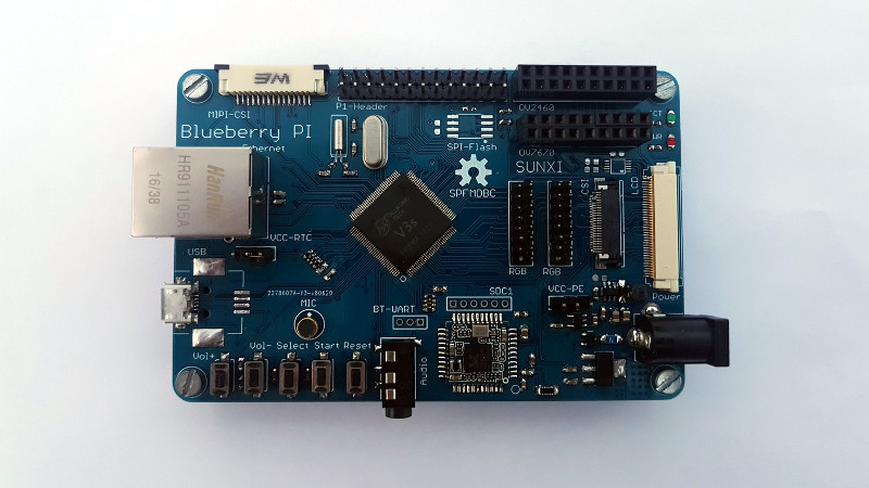
[Marcel Thürmer] may have managed that feat, with his Blueberry Pi. On the face of it this is just Yet Another SBC With A Fruity Pi Name, but what caught our attention is that unlike all the others, this is one you can build yourself if you want. It’s entirely open-source, but it differs from other boards that release their files to the world in that it manages to keep construction within the realm of what is possible on the bench rather than the pick-and-place. He’s done this by choosing an Alwinner V3, an SoC originally produced for the action camera market that is available in a readily-solderable TQFP package. It’s a choice that has allowed him to pull off another constructor-friendly feat: the board is only two layers, so it won’t break the bank to have it made.
It’s fair to say that the Allwinner V3 (PDF) isn’t the most powerful of Linux-capable SoCs, but it has the advantage of built-in RAM to avoid more tricky soldering. With only 64Mb of memory, it’s never going to be a powerhouse, but it does pack onboard Ethernet, serial and parallel camera interfaces, and audio as well as the usual interfaces you’d expect. There is no video support on the Blueberry Pi, but the chip has LVDS for an LCD panel, so it’s not impossible to imagine something could be put together. Meanwhile, all you need to know about the board can be found on its GitHub repository. There is no handy OS image to download, u-boot instructions are provided to build your own. We suspect if you’re the kind of person who is building a Blueberry Pi though this may not present a problem to you.
We hope the Blueberry Pi receives more interest, develops a wider community, and becomes a board with a solid footing. We like its achievement of being both a powerful platform and one that is within reach of the home constructor, and we look forward to it being the subject of more attention.


So I’m guessing there are no mystery binary blobs in this project like found in ther raspberry Pi so that’s good. I also assume the usb port there could be connected to usb devices like another ethernet port or wifi adapter. If so, this could be a useful low-end router with zero “mystery” components leading to high security levels if configured correctly. Interesting, but ther 64Meg ram limit hurts.
as far as I know the blobs for RPi are for the VideoCore GPU and bootloader. There is an effort to implement an open replacement for VideoCore. I’m not sure about bootloader yet. It seems like a pretty simple bootloader, I suspect it’s a lack of interest rather than a lack of information?
Thanks for the reply. Blob-free computing apeals to me. One doesn’t always have a fire extinguisher handy. (referring to “The Blob” the classic cheesy 1950’s movie that in my humble opinion, everyone should see once)
Yea, sometime I live by the code:
“I’m afraid of not being paranoid.” – Most foxes are that way. :-)
meybe using FPGA to code CPU and Core Video?
Lack of binary blobs loaded by the user doesn’t imply there couldn’t be entire hidden parts and code on the chip, though.
Good point. It still comes down to whether you can trust the manufacturer, and if it comes out of China…. I guess there is always the fine layer teardown and electron microscope reverse engineering technique that could verify design compliance but that still wouldn’t work because that method only tests devices that you have already destroyed, not the specific one a soul might try to use. Yea, I know, excessive paranoid mode again. :-)
Meh…
I think given the actions of both nations the question of which can be trusted is a very obvious neither.
Its all a poker game or game of chicken. (take your pick) It’s all about making the right deal. There’s bluffing to do with possible folding or calling. You go for the bridge or you faint away. Trust has nothing to do with it unless you can verify.
An SBC with the V3 exists already (the LicheePi Zero ), so does near mainline Linux and modules for a lot of functionailities. 64MB was enough to get lighttp running and serve websites, but without fastCGI.
The Allwinner V3 was made for Dashcams, this is why you find a decent GPU, camera and display interfaces and built-in RAM.
Not so easy to buy. Where is this licheepi sold ?
64MiB enough to serve websites? What a bloated world we live in…
Exactly Megol this is part of the reason why internet is so slow today compared to telephone dial up days, handicap webmasters today put on a 80,000 * 60,000 pixel picture straight from the camera on their server, then use HTML code to chop the picture down to a small 80 * 60 pixel picture.
How is it achieving impedance matching for Ethernet and USB lines on two layers?
The usual ways?
Normal balanced lines with groundplane on the other side.
At least that’s what it looks like on the pictures as I’m yet to take a look at the board files.
Except … no. Looking at the Gerbs, there is no continuous ground plane under either the USB or the Ethernet lines. So they may just be pretending these are balanced transmission lines, which they really can’t be, with as much crap as there is routed so close to them. This kind of lowers my confidence in the design.
What could happen outside of some lost packets that would need a resending?
Well, for one thing, EMI.
>Well, for one thing, EMI.
If in doubt enclose it in a metal case connected to GND and call it a day.
Hackers don’t make stuff that is “correct”, they make stuff that works (most of the time). Running stuff out side the stated voltages, leaving out parts to make it easier to build, ignoring design rules and never considering things like EMI is the order of the day. If you want ‘how to make a commercial product’ that will pass all regs you need to look else where. Again, this is a hacking site, not following the rules is the only rule.
Only to the point it doesn’t cause problems for ourselves, or others. I’m sure the Hams know this.
“Again, this is a hacking site, not following the rules is the only rule.”
Considering the number of my posts that have been deleted by HaD editors, there are a number of RULES.
That’s a rhetorical question for anyone that have some PCB backgrounds. You can’t do it on 2 layers 0.062″ as the tracks would be like it was drawn with crayons (i.e. thick).
The only thing you can do is to keep the tracks short enough to not mess it up to much. You may lower the impedance a bit by edge couping effects, but that’s not gong to get the right values either for odd/even modes impedances.
Sounds like a good idea for someone to make a pull request with an updated multilayer board. It’s open source after all.
Not as cool as CP/M on a z80 circuit
Cool project, but you’re right. I already built a z80 that can run CP/M and defined for myself that a self-made computer is not putting a module on a breakout board. You made a computer by yourself if you put together RAM, ROM and the CPU, everything else is a breakout board for a computer that you just bought.
“I already built a z80 that can run CP/M”
Video or it didn’t happen.
Just kidding, but more details please!
B^)
Yay! CP/M forever!!!
64K should be enough for anyone!
>With only 64Mb of memory, it’s never going to be a powerhouse,
If you can’t keep track of proper usage of units using the right capitalizations, you should consider spelling it out like the article. 64Gb is 8 times less than 64 gigabytes. As a tech writer, you should know better.
The article said:
>The V3s is a very unique SoC, it can be called the true 3 in 1 chip solution. Beside the ARM Cortex-A7 @ 1.2GHz, the V3s has built-in 64 Megabyte of RAM and an Ethernet PHY.
What exactly does “8 times less” mean? If A is 8 times less than B, then doesn’t that mean A = B – 8 * B = -7 * B? Because that’s what the words mean.
To expand on this a bit: if you say that something is “25% less”, this means 100% – 25% = 75% of the original value. Which makes sense. Now, even simpler, what does “50% less” mean? It means 100% – 50% = 50%. Nobody has a problem with this. Now, what does “200% less” mean? Oh. I guess it means the same thing as 50% less, by no possible train of logic. So by saying “8 times less”, that would be 800% less. In actuality, you mean “1/8 as much as”, which is equivalent to 7/8 less, not 8 times less.
lol
I love the comment section
8 times less means that you have a number (or something else) and divide it by 8 (you separate it to 8 identical groups and take one of the groups). For example if you have 8 times less then $8, you have one dollar. I don’t know which school you graduated but he here in the middle Europe learn these staff in kindergarten (preschool education).
Sorry for my bad English, it is my third language and I am not talented in languages. :)
There are 8 bits in a byte. 8 Megabits in a Megabyte. So it makes a difference if you are talking about megabits or megabytes. If you mean megabytes then that is 8 times the size of a megabit, if you are talking about megabits then that is 1/8 of the size in megabytes.
But what if a parity bit is used, making it a 9 bit byte?
It’s not counted in the totals and instead you just have ECC RAM.
… Then the RAM chip manufacturers try to sell it as a “72 megabit” chip and not a 64 Mb one. They all use ‘megabit’ and basically never ‘megabyte’ anyway — gotta make it look bigger than it really is. (same rule for HDD manufacturers, who suddenly (for the industry) spontaneously all chose to adopt the correct SI meaning of the prefix ‘Mega’, ie 10^3, rather than the 2^20 that even those chip manufacturers use. And “actual formatted capacity may be less”. (although, RAM chip have good reason to use powers of two: Address lines only come in natural integers where devices use them, and by definition, a RAM chip pretty much has to be an array of some sort. (not so flash memory, but I’ve already digressed enough :)))
damn – posted in the wrong spot. Anyone else often have this site just time out trying to post? (or authenticate such as with wordpress or google?
Was answering the question of what happens with 9 – bit bytes.
BTW you can also get SRAM chips with 18 bit ‘bytes’ – really just memory bus width, so it does make some sense to compare by megabits.
Whatever the author meant by 64Mb, it tells me that the chip has a lot less memory than a number of chips out there.
Whether it is 64 Mb or 64MB, there is probably a version of Linux that will run on it… and probably no version of Windows B^)
I don´t want to be mean or something but..
1) USB and ETH traces are not length matched
2) 2L design is kinda bad thing with high speed connections, and having inconsistent ground on other side is not good for RLC parasities also
3) Where is RAM? :D you know that 64Mb RAM is waaay too small
4) Crystal signals aren´t again length matched.. i am surprised it worked
Currently i am working on A10s dev board with 1GB external RAM, SATA connector and HDMI (pretty sensitive stuff) and you cannot just route it as you want, at 533MHz speeds, one signal could (and probably would) arrive sooner that other, CPU will got confused and probably it wont even work.. I mean like.. it doesn´t look bad from pictures, but when i dug down schematics and layout.. nah mate, a lot of reading and rework to do, sorry. BTW i strongly recommend you Altium, KiCAD or OrCAD for better design experience, since Eagle doesn´t have length matching (actually it have diff. pair routing, but it´s kinda shite)
Well this IS a technical forum. What other kind of discussion is there?
Just what I’ve been looking for. :) Been itching to design my own SBC.
Don’t ask why, ask how.
Why?
How?
When?
What?
WAFFLES!
do this with the octavo systems Beagle SiP for more fun and more power
This is TQFP instead of BGA like the Octavo SiP.
Not that the Octavo SiP is a dense bga, it has wonderfully long distances between the bga balls making it very hobbyist compatible.
But not as compatible as TQFP :)
How so? Do you mean peripheral-wise?
The A7 is the 28nm evolution of the 65nm A8. It has some pipelining simplifications that result in slightly lower DMIPS/Mhz. But higher clock rate and more cache that should make it perform better than most any A8.
A lot of OpenWRT modules are similar in features to the V3S. However I don’t believe any come close to memory in package (vs in module). The Renesas RZ/A1x is interesting – QFP + up to 10 MByte SRAM in package.
Cool chip
I’m surprised there’s no talk about reusing boards from commercial products. My found in a recycling bin DVD recorder uses Linux, and it no longer has much use because It doesn’t receive DTV. My blu-ray player uses Linux, as does both my TV sets. My TomTom One GPS uses Linux too.
Probably there are limits due to too little memory and lack of I/O, but it’s interesting that small Linux boards are so close. Junk electronic equipment didn’t have that when I was a kid.
Michael
Cheap routers as a ready source of Linux SBCs.
Imagine what the future might hold!
In all seriousness, I commonly use android phones and android STBs for anything that needs a little more oomph, a built in battery, or wifi capability.
If binary blobs upset Raspberry Pi people, then Android phones will make it worse.
Seems moot as the latest Kernel 4.18, for Linux specifically supports the Pi B and B+
https://www.omgubuntu.co.uk/2018/08/linux-4-18-kernel-release-features
FYI, here’s the real datasheet for the chip: https://github.com/petit-miner/Blueberry-PI/raw/master/Hardware/Datasheets/IC/Allwinner_V3s_Datasheet_V1.0.pdf
I’m also working as a hobbyist into a SBC/arm based device. It have an Allwinner A33 soc.
Right now I’m into the design phases.
https://hackaday.io/project/159654-fcthermostat-another-overengeneered-iot-device
Good stuff, specially coming from a hobbyist. Hand-solderable IC’s are hard to come by (unfortunately), and the trend says it will become harder in the future; good to see someone invest effort and time to develop a base-board this powerful
Just cottoning that it’s got pretty much everything included in the one chip… giving me crazy ideas about deadbugging one into one of those super cheap chinese “smart watches” that are more of a glorified bluetooth accessory and making it actually kinda smart….
Any recomendation if I am looking for interested guys to help me in an very interesting project that can be very (with emphasis on very) lucrative in the end. It involves design of a SBC (with an onboard FPGA), porting from raspbian to Ubuntu or similar , HD video, WiFi transmitting, cloudbased statistical analyses if data.