When current flows through a conductor it becomes an inductor, when there is an inductor there is an electromagnetic field (EM). This can cause a variety of issues during PCB layout if you don’t plan properly, and sometimes we get burned even when we think we have planned for unwanted inductance and the effects that come with them.
When doing high speed logic we need to be able to deliver sudden changes in current to the devices if we want to have proper switching times and logic levels. Unfortunately inductance is usually not a friend in these circumstances as it resists those sudden changes in current. If the high speed devices are driving capacitive loads, which themselves are resisting changes in voltage, even more instantaneous current is needed.
Simply put, inductors resist a change of current, and can act as a low pass filter when in series with the signal or power supply flow. Inductors do this by storing energy in the flux surrounding the conductor. Alternatively capacitors resist a change in voltage (again by storing energy) and can act as a high pass filter when in series with the signal. This makes them a valuable tool in the fight against unwanted inductance in power supply distribution.
In the video below, and the remainder of this article, I’m going to dive into the concept of inductance and how it affects our design choices when laying out circuit boards.
It may be something you’ve never considered before, but the electrical properties of PCB traces matter a lot as electronic components continue to increase in speed. Resistance in the traces results in voltage drop and also slows the charging of capacitive loads. Inductive Reactance (XL), which can be thought of as a frequency dependent resistance when it comes to supplying current, further complicates our design challenges. But having a basic understanding of what we’re up against will help you recognize problems while designing, instead of after assembling your prototype boards.
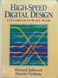
Here you can see three of my favorite books which are a great resource if you want to take a deep dive into these topics. In the video I walk through several topics from these texts, beginning with DC resistance in traces which ultimately result in the table below. You can see here that an inch of an average PCB trace can have between 0.1Ω and 15Ω of impedance depending on frequency or risetime of the signal. If we plug the impedance into Ohms law, we see that 10Ω at 0.1A is a 1V drop in voltage.
| Frequency (MHz) | Rise Time (ns) | Impedance (Ω) |
|---|---|---|
| 1 | 318 | 0.1 |
| 10 | 31.8 | 1.0 |
| 30 | 10.6 | 2.8 |
| 50 | 6.4 | 4.7 |
| 70 | 4.5 | 6.6 |
| 90 | 3.5 | 8.5 |
| 110 | 2.9 | 10.4 |
| 160 | 2.0 | 15.0 |
Knowing that voltage drops in circuit board traces are usually unwanted, we can conclude that inductance in those sames traces is also therefore unwanted. Consequently the more inductance there is, the worse the effect it has on our circuit.
What may not be intuitive to all is that the larger of a loop of conductor, the larger the Inductance. In other words, the larger the area inside the loop formed by the power and ground return paths, the higher the inductance, the higher the resistance to high speed demands for current.
After years of knowing this relationship, but not knowing the specific formula for calculating, I found this formula in the book High Speed Digital Design:
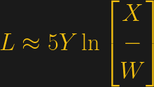
The formula shows inductance as a function of area using the variables as follows:
- L = Inductance
- X,Y = Dimension
- W = Width of conductor
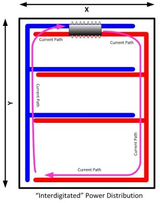
Simply put, power and ground return paths should be as close together as possible. This minimizes inductance and limits the consequential voltage drop and helps to preserve fast changes in current in response to demand.
Knowing this you can see just how bad a common practice used on some prototyping boards, known as “interdigitated” , really is. You will often see a voltage bus on one side of a protoboard and a ground bus on the other (as is shown below). In effect the power supply loop area is close to the size of the entire board. Increasing the width of the conductor doesn’t really lower the overall inductance much due to its place in the equation. The best answer is to reduce the size of the area by techniques such as creating a grid of the power and ground paths or through judicious use of ground and power planes.
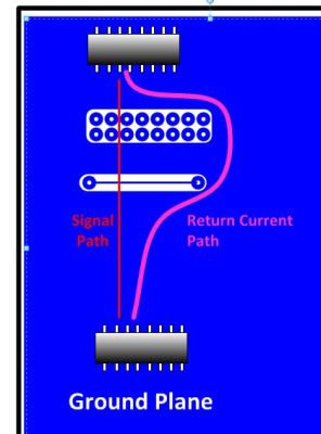
Using a ground plane doesn’t automatically mean that the inductance problem is minimized; care must be taken to not inadvertently create problems by placing obstacles on the ground or power layers. As the frequency of the signal goes up, the closer the return path will follow it on the ground (or power) plane. If the signal goes through a gap in the plane, such as might be created by a connector or routing a signal trace on a plane layer, the return path may have to take a detour, which increases the loop, sometimes unexpectedly.
An example of how the return path can be affected by a hole in the ground plane is shown. In practice the ground or power plane is often buried, making this issue may not be readily visible. Cross talk can also become an issue if two singles end up squeezing through the same small area between two obstacles.
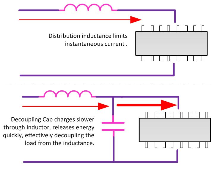
You are likely familiar with decoupling capacitors, those ever present little capacitors that tend to hug the Integrated Circuits (ICs) and straddle the power supply as close as feasible to the IC itself. The idea is that the inductance in the power traces still exists, but there is a source of current close to the IC which results in much less inductance between the decoupling capacitor and the IC due to proximity.
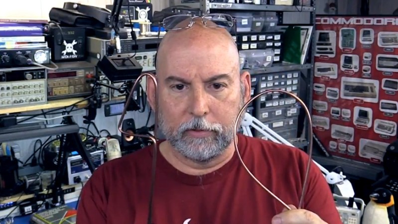
Finally, you should become familiar with the effect of an “inductive kick”. This is demonstrated in the video in the same was I learned about it when I was a kid. I briefly light up a nixie tube with a big ‘ole coil and a 9V battery. The demonstration is meant to show that inductors really do dislike a change of current, and use the energy stored in their flux to keep current flowing, even to the point of creating over 100 volts needed to ignite the nixie.
Knowing the basics of inductance and capacitance are crucial for PCB designers. You already know that ICs need decoupling capacitors, but knowing why is a better nugget of knowledge. Knowing some of the gotchas that await poorly routed high-speed traces will save you a ton of time and headaches.


39 thoughts on “Inductance In PCB Layout: The Good, The Bad, And The Fugly”
Leave a Reply to MacCancel reply
Please be kind and respectful to help make the comments section excellent. (Comment Policy)


This is so much good stuff! Looking forward to later in the day when I can watch the whole video and read more carefully.
The latest edition of Ott’s book has been renamed “Electromagnetic Compatibility Engineering”
It’s quite a good read (although the first few chapters that rehash electromagnetics fundamentals are a bit dry).
I’m currently reading the latest edition of Morrison (Grounding and Shielding: Circuits and Interference) and I must say that I prefer Ott.
Yeah I have the new edition you mentioned on my Kindle, but I have a fondness for the little grey books.
Ott’s book is the bee’s knees, but this is also great condensed information. I’ve been toying with the idea of making a video with horrific layout vs. EMI conscious layout and compare them inside of my TEM cell to visually see the difference. I’ll get around to it someday!
Plus something like that never seems to go the way I planned, its hard to intentionally do something wrong.
I always see that picture going around of curved traces, vs. 45 deg traces, vs. acute bends – stating that tight bends are the worst. I would really like to test out how bad it really is… I made a trigger w/ pretty fast rise time for that purpose, I just can’t find the personal time to do it!
For the most part, it’s the same effect as putting a capacitor on the line because it’s the extra copper that matters. For a 90 degree bend, it’s like putting a 1.6 fF/mil width capacitor there if you’re on FR4 with a 50-ohm microstrip line (because you’re adding about a half line-width extra capacitance, and the capacitance is 3.3 pF/in). So a 10 mil width trace adds 16 fF capacitance.
How much that matters obviously depends on the frequency. At 1 GHz, it’s got 1 kOhm impedance to ground, against a 50 ohm impedance, so it’s a few percent reflection.
https://www.edn.com/electronics-blogs/all-aboard-/4438573/When-to-worry-about-trace-corners–Rule-of-Thumb–24
Yes, if you where to take a 90 degree corner and straighten it you would have a straight trace with basically a triangle stuck on the side. The increase in width amounts to a change in impedance and can result is a certain part of the signal being reflected. More so a bunch of corners can have an accumulated effect.
For slow moving signals like I/O lines there usually is no big concern with 90 degree corners.
Regarding teardrops on pads, while they may look like they allow a “smoother flow”, they are really there to increase the yield on PCB manufacture as it allows the hole to be slightly off-center sometimes, depending on the orientation.
See the Doctor’s article, “Who’s afraid of the big, bad bend,” at https://web.archive.org/web/20110910025458/http://www.sigcon.com/Pubs/edn/bigbadbend.htm .
is the Ott still very expensive? when I was at uni many years ago it was something like 2-3x he price of the other books I had to get
I think I got my new old one off of ebay or used off amazon. Back in the day it was a weeks salary for a lowly engineer so we had a department copy we would share.
I bought it in the early 90’s I think it was $140
“A Handbook of Black Magic” indeed. I have so much respect for people who understand this stuff on a higher level.
I tend to shy away from the term “magic” because I have seen management misuse the term, I tend to prefer the term “art/arts”.
Harry Potter uses magic too, but he takes the time to study it and figure out how it works. That’s how you stay in control of your designs.
You’re mistaken. Hermione studies and figures out how it works. Harry just relies on talent, brute force, and luck.
And on Hermione, if it turns out that none of his shit works.
Great video Bil!! Always excited to watch these.
There is also some good stuff on high speed routing in the Xilinx documentation about routing differential pairs and controlled impedance traces.
Yeah the FPGA companies have stepped up with their documentation regarding the environment that the parts live in. I try to hit on that a bit in the post https://hackaday.com/2016/03/29/when-difference-matters/, there was no shortage of info available.
Nicely done. Thank you.
I particularly like that you tied it into decoupling caps.
2 of those books are available on the internet archive, unfortunately not Henry Ott’s.
Also, check out Lee Ritchey’s ‘Right the First Time’ book online with free donload. Explains a lot about high speed design.
http://www.thehighspeeddesignbook.com/
TIA Mr. Ritchey
The interview with Ritchey at the above ink is worth the time to view. Then it may to be for visitors to Hackaday, as he doesn’t celebrate the typical hacker ethos, as the book title should suggest.
Now if he could add a feature to blow a hole through the poachers he might have something…
Great presentation Bill, thanks for taking the time to produce it.. No doubt there are good videos on you tube that illustrate why both capacitance and induction exist. When bench racing with a group where I was outnumbered computer geeks at the time when computer speeds where rising, I mention the board designer are going to have their thinking caps on straight, I was dismissed, because I was that electronics and electricity guy. Fine; my skin is thick enough, I can take it. This video informed to that I didn’t have a clue as to how correct I was.
When I was getting started in this stuff, some engineering students went into digital to avoid the heavier math of analog; but as speeds increased, digital became the worst form of analog—RF and microwave!
Funny reading this. We had a project with a distributed clock signal. Everything was daisy chained and in theory, it worked. They fired up the system and the clock was missing on a couple of units. Told the engineer ‘the cable is way too long.’ He ignored me and began troubleshooting the system. Next thing he pulled out the cable and laid it on the floor. A quick tape measure check of the cable and some fast calculations had him cursing. It was 1/4 wavelength long and the length was such that it hit the current node. No signal. He looked at me and said ‘how did you know before even looking at it?’ Told him ‘I saw it being assembled and the individual assembling it did not want any help.’
I am big on “detuning” traces, and mention that in one of my FPGA videos that I hate stubs, even short ones, and try and make all power traces into a loop. I have seen “standing waves”, that point in the trace where the interference from reflections consistently occurs, have very real effects. On the C128 there is a single wire on the PCB that is redundant to the A10 signal already present, which we ran for when the Z80 was talking to DRAM. In this case there was a glitch standing right at the address MUX to the DRAM, adding the wire removed the reflection as there was not stub to reflect from.
The worst thing I saw was many years ago, a spiral formed by the power trace on a plug in options card. The other engineer swapped out the NMOS EPROM for a CMOS one and it didn’t work. I asked to take a look and started removing all other chips while testing the EPROM in a loop. With the CMOS EPROM being the only load, on an 8″-10″ trace (in a spiral no less, it probably didn’t really make the problem worse, it just showed not to take short cuts on option boards either) and it rang like a bell! 4V oscillation on the 5V power trace! The NMOS drew enough current to terminate the end of the line, the CMOS was like a feather. A wire from the end of the line to the entry point on the board changed the symptoms in a way that allowed it to work.
I realize this particular article focuses on digital, but, the role of inductance in less digital designs should not be underestimated. Just try to design a good switching power supply while ignoring these concepts…
True,thise post was only about unwanted inductance in PCB layout, I had previously talked about transmissions lines for example, where inductance combined with capacitance creates a transmission line which is a reliable way to transmit digital and analog/RF signals when done correctly.
I worked in UHF power transistor applications engineering in the mid 1980’s, and can tell you most electronics enthusiasts have absolutely no idea what goes on there. What may be surprising is that my understanding of high-frequency behavior has further increased dramatically from working in digital and even switch-mode power supplies where the rise times are not particularly impressive compared to digital but the di/dt’s are astronomical.
Good article, and a critical topic for anyone doing real-world board design. Discussions like this are a great jumping-off point to thinking about things like EMC/EMI.
I think it’s worth clarifying, however, that the approximate formula for loop inductance presented in the article and the video is valid only in the context of certain layouts (such as grid or interdigitated layouts) where “X” and “Y” have clearly defined physical meanings (in the more general case of a single trace in a rectangular loop, you can see how the selection of which dimension is X would affect your result). I haven’t read through High Speed Digital Design, but I have spent some quality time with a more recent edition of Ott’s book (“Electromagnetic Compatibility Engineering”, also recommended by a couple other commenters) and it lays out some approximations for calculating mutual/self-inductance in various physical scenarios. Long story short is that in the real world it gets really complicated, fast.
Thankfully, though, for many aspects of practical EMC/EMI I’ve found that it isn’t especially important to be able to calculate the inductance of a particular trace. As Bil gets into near the end of his video, what’s *is* important is to be able to reason about the paths current will take through your layout at the frequencies that will be present in your signal. If you can do that, you can then apply the tools at your disposal – inductors, capacitors, and layout – to adjust those paths at various frequencies to reduce emissions and noise without impacting the fundamental signal of interest.
Mostly HaD is entertaining, but sometimes it’s educational too! Thank-you! I count three things I learnt in five minutes and I didn’t even watch the video or read the book.
I have seen basic inductance measuring kits, typically running under 1MHz. What methods are best, as you go up in frequency?
I suspect it gets hairy checking a PCB trace at hundreds of MHz.
For PCB traces its sort of complicated as there are many points and different sources all happening at once, I.E> its not a simple inductor and we are often concerned with what happenes at various lengths down the conductor.. There are expensive simulators but they ultimately are best mathematical guesses.
There are tools meant for RF like a Vector Network Analyzer that may offer insight but they are expensive also. A grid dip meter held in parallel can sometimes give a clue in simpler situations and it is that frequency source you mentioned, but you have to couple it to the circuit under test. Its actually pretty good at ferreting out resonant circuits and the like where if you know the capacitance (or at least a guess) you can start to make some assumptions about the inductance.
YES! Another video from BIl. Thank you!
Yep – I have all three of those books – and each are well used and well worn! Good examples with the PCB image current visualization.
Here are a few videos I did on related topics:
Power supply decoupling: https://www.youtube.com/watch?v=9EaTdc2mr34
Inductive kickback (relay coils): https://www.youtube.com/watch?v=c6I7Ycbv8B8
Self-resonance of caps: https://www.youtube.com/watch?v=vi24SpKYYoQ
Scope Probe ground lead inductance: https://www.youtube.com/watch?v=zodpCuxwn_o
Homemade high-performance probe socket: https://www.youtube.com/watch?v=-4q8geE5ef8
We had a large (for space flight) box on Skylab that had multiple clock signals distributed to provide clocking to avoid race conditions and we found that the 64ls series of Ics would go crazy if the clock signal went negative. Routing the clock line around the chassis caused the problem and we had to terminate the line with termination to snub out any ringing. The production people balked at running the clock line in such a controlled way but it soved the problem.
I’ve been laying out boards for 30 years… you cleared up a lot of answers for “why” I do what I’ve been doing in a very easy to understand and concise way. Very cool dude… thanks for sharing! Keep it up!