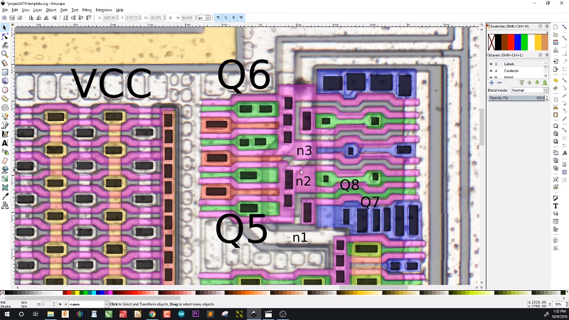
ICs have certainly changed electronics, but how much do you really know about how they are built on the inside? While decapsulating and studying a modern CPU with 14 nanometer geometry is probably not a great first project, a simple 54HC00 logic gate is much larger and much easier to analyze, even at low magnification. [Robert Baruch] took a die image of the chip and worked out what was going on, and shares his analysis in a recent video. You can see that video, below.
The CMOS structures are simple because a MOSFET is so simple to make on an IC die. The single layer of aluminum conductors also makes things simple.
One disadvantage to working with a picture is you can’t etch off the passivation — the thin layer of glass over the top of the chip — and then remove the aluminum to see underneath. However, there isn’t much going on in a chip this simple and you can usually see outlines of contacts under the aluminum.
At this scale, it is possible to put the part under a microscope after removing the passivation and actually probe or even cut conductors with a very sharp probe. The probes are typically made from wire sharpened electrically using sodium hydroxide. Of course, that’s a nasty chemical and so is the hydrofluoric acid that takes off the glass.
One of the hallmarks of CMOS is that you have two transistors driving a signal. One drives it high and another drives it low. Some other logic families will only have one type of transistor, usually pulling a signal low and rely on a pull-up resistor for high outputs. This is why some logic families can “sink more than they source” and also explains higher current consumption and heating. Also, accurate resistors are not easy to make on a chip. Usually, they are made of highly-doped semiconductor material or polysilicon and the actual resistance can vary quite a bit from part to part.
If you’ve ever wondered what’s behind the curtain, [Robert’s] video is pretty lucid and easy to understand. After you watch it, we have a challenge for you: look at a relatively simple 8088 CPU die and imagine doing the exercise on that. Now, look at a really modern CPU. With practice, you can pick out zones pretty easy (registers, an ALU, and so on).
It used to be this kind of thing was what people did in reverse engineering and failure analysis labs, but we are seeing more and more of it lately. We used to decap chips with fuming nitric acid, but there are other methods. If you get the old packages with the gold lid, a hobby knife will do the trick if you are careful.


waiting for some computer vision software that can reverse-engineer microphotos or x-ray tomography into an actual circuit … that might bring the golden age of opensource hardware to the die level.
That’s been a dream for a long time. We worked on a system in the 80s that could compare a good part to a bad part using electron stroboscopy to image the electrical signals on the part. A high energy secondary electron meant – potential and a low energy one meant + potential. Shoot that a few thousand times at the same point at the exact same point in a loop and you can decide the voltage at that point. Now scan in the XY position and you can build an image. Now slide your time reference and you can make a movie. High tech in the 80s with a computer the size of a deep freezer.
Hmm, could we re-engineer a suitable variation of 3D printer paradigm with the appropriate materials multiple extruder wise and even though coarse at first to achieve the same on an as need basis tucked away inside the surfaces of product enclosures where feasible for example ?
A satellite containing a chemical photo lab exists (https://hackaday.com/2018/08/02/the-photo-lab-that-flew-to-the-moon/) and making chips is similar although with more steps, so it should be possible to automate. It’s not possible to do with purely additive manufacturing since it requires etching ion injection (maybe also sputtering and electroplating).
inkjet printing is showing a lot of promise for additively manufactured electronics, including FETs.
But probably magnitudes away (lower) from the precision and performance of present CMOS technology.
It’s certainly good in understanding all that stuff the professor taught in a practical setting.
Comparing NaOH (sodium hydroxide) with HF (hydrofluoric acid) is strange. While the NaOH is strongly corrosive it’s not really toxic and the main components of most drain cleaners. HF is a very strong poison.