In a recent video, [Andrew Zonenberg] takes us through the process of decapsulating a PIC12F683 to take a peek at its CMOS implementation.
This is a multipart series with five parts done and more to come. The PIC12F683 is an 8-pin flash-based, 8-bit microcontroller from Microchip. [Andrew] picked the PIC12F683 for decapsulation because back in 2011 it was the first microcontroller he broke read-protection on and he wanted to go back and revisit this chip, given particularly that his resources and skills had advanced in the intervening period.
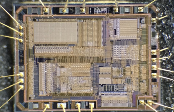
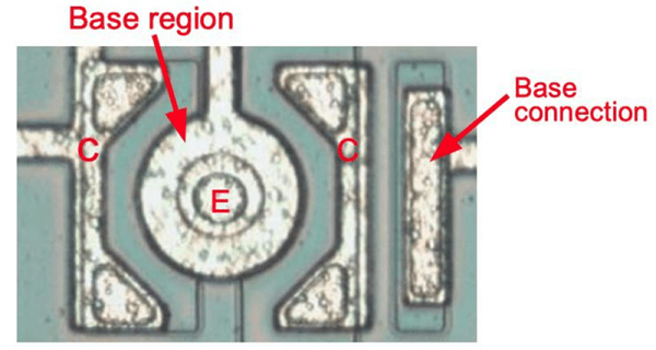
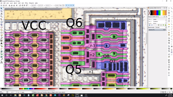
The five videos are a tour de force. He begins by taking a package cross section, then decapsulating and delayering. He collects high-resolution photos as he goes along. In the process, he takes some time to explain the dangers of working with acid and the risk mitigations he has in place. Then he does what he calls a “floorplan analysis” which takes stock of the entire chip before taking a close look at the SRAM implementation.
If you’re interested in decapsulating integrated circuits you might want to take a look at Laser Fault Injection, Now With Optional Decapping, A Particularly Festive Chip Decapping, or even read through the transcript of the Decapping Components Hack Chat With John McMaster.
Continue reading “Decapsulating A PIC12F683 To Examine Its CMOS Implementation”