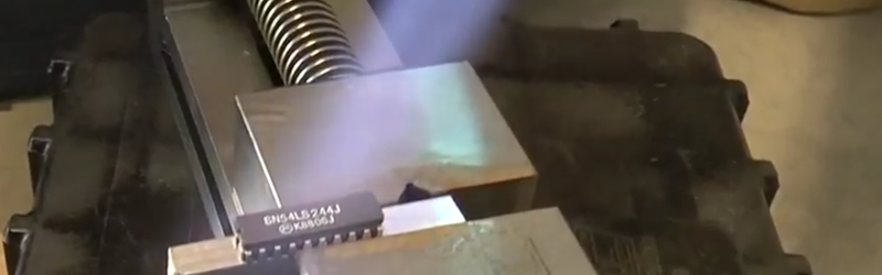
If you’ve ever wanted to open up an IC to see what’s inside it, you have a few options. The ceramic packages with a metal lid will succumb to a hobby knife. That’s easy. The common epoxy packages are harder, and usually require a mix of mechanical milling and the use of an acid (like fuming nitric, for example). [Robert Baruch] wanted to open a fully ceramic package so he used the “cooler” part of a MAP gas torch. If you like seeing things get hot in an open flame, you might enjoy the video below.
Spoiler alert: [Robert] found out the hard way that dropping the hot part isn’t a great idea. Also, we are not sure what the heat does if you want to do more than just inspect the die. It would be interesting to measure a junction on the die during the process to see how much heat actually goes to the device.
The process is really fast: only about 20 seconds. We wondered if a larger part might take a little longer. However, compared to chemical methods, this looked very fast and easy, as long as you don’t mind the heat.
If you get the urge to start opening parts and want to actually probe the surface of the die, don’t forget there is a thin layer of glass over almost the entire chip. This layer–the passivation–is relatively thick and usually only has cutaways around the bonding pads. Getting rid of that layer requires hydrofluoric acid (nasty stuff). You can tell when you got it all by focusing a microscope up and down the edge of bond pad. When you can’t find the edge of the passivation, you are done.
Some people expose ICs dies to study, and some are looking for fake chips. Other times, it is electronic archeology. The last time we saw [Robert] he was building a CPU on an FPGA, so he’s clearly a hacker of wide-ranging interests.


Did anyone else read that as “Pooping on Top of A Ceramic IC” ;)
The rest of the Hackaday community is not as nasty as you man. Take it easy on the pills.
Nah man, I saw the same thing, just didn’t want anyone else to think I did.
2 Breadboards, 1 IC … nnnnnoooo make it stop!!!
Once you poop the fun don’t stoop.
Seems like a lot of work. Last time I did this I just laid the package on its side on a piece of scrap wood and put a wood chisel (that I didn’t care much about) on the glue line and one nice rap with a hammer and it cleaved right open. Like the hollywood image of the guy splitting a million dollar diamond. Ceramic packages are easy.
We used to just pop them open by using a pair of diagonal cutters on the cement joint. Usually, the top would pop right off. My first job in 1974 was opening and photographing Fairchild ICs for the second sourcing work at IT&T Semiconductor. Really.
I should really just bite the bullet and try the chisel. I just use the flame approach because I don’t care about a live die, and I have a failure rate (where I ruin the chip) of zero.
In electronics school, the new students used to pop the top off of ICs, by applying way too much voltage, or shorting things out in the circuit.
Reminds me of a story about somebody putting an EPROM backward into a prom burner. He was admiring this little red pilot light under the window, then it struck him that something wasn’t right.
Haha, EPROM as an LED replacement.
We used to joke about Smoke Emitting Diodes…
Color-changing LEDs. Though only for a second or two. ;)
LEPROM
Perhaps LENPROM
Light Emitting Non-Programmable Read Only Memory.
Write-only memory… for you sure aren’t reading it back!
They must have been using a cheapass EPROM burner as most decent ones have current limiting on all pins.
Rather than a chisel, I used a small drill bit and a vise. There’s less chance of damaging the silicon or the bond wires that way.
Take a drill bit that’s just slightly thicker than the width of the glue line.Place it along the short edge of the chip on the glue line, and clamp them both together in the vise. Tighten the vise to force the drill bit into the glue line and the top will pop right off cleanly
My final year project was an interface bus board for a minicomputer in the Electronics department; it would protect the computer from any student projects, by giving them an isolated bus to plug in to. To demonstrate it worked, my professor got me to hook up a board for programming EPROMs (2708s) and to write some programming software for students to use. If you forget the 50ms delay in the main loop, EPROMs light up like a candle.
But the only time I have ever automatically de-lidded something was a power transistor in a TO3 case. One went *foom* and the lid – this tiny flying saucer – went past my ear, leaving two posts and a small charred square.
Next step: swapping the tops of different chips and returning them to storage. Example, hex buffer and hex inverter.
I hope he’s not annealing that nice vise too much.
We use to put pictures on the die’s. I think it was a form of copy protection, but not sure. Stopped doing it because silicon real estate was too expensive.
The way I did it was to put the chip lengthwise between the jaws of a bench vise at a slight angle so that one jaw is pushing the top one way, and other is pushing the bottom the other way in shear, and then tighten the jaws. The halves separate cleanly.
Why do you want to pop the top off when you know whats inside?
I used to take things apart when I was a child and learned alot from that.
But chips, why?
To add them to a Silicon Zoo, or even just to check for Chip art.
Obligatory:
That’s not “MAPP” (methylacetylene-propadiene propane) gas. That’s “MAP/Pro” which is actually propylene gas. MAPP gas has not been sold in the US since 2008.
Be careful about this folks. I once wanted to see inside of an MRF151 RF transistor to see if I could determine exactly what had failed in the device. At the time they were running about $150 each. The transmitters I worked on contained about 240 of them, so the exact cause of failure was reasonably important. I though I’ll just grind the top off…. White ceramic… Suddenly realized that I was grinding on beryllium! No dust mask! Needless to say I immediately quit what I was doing. Just luck I didn’t get a lung full of beryllium dust! NEVER GRIND ON WHITE CERAMIC!
That is an extremely good point! They are not dyed pink and alerted with a nearby warning sticker like in x ray machines and some commercial microwave ovens.
Yes, very good point! BeO (Beryllium oxide is HIGHLY TOXIC!) https://en.wikipedia.org/wiki/Beryllium_oxide
Tiny TTL ICs are relatively uninteresting compared to EPROM silicon. I used to find broken EPROMs in the trash at an arcade warehouse and they looked like a Terminator chip.
> Getting rid of that layer requires hydrofluoric acid (nasty stuff)
*Very* nasty stuff, can easily kill people if mishandled, deaths are usually prolonged and unpleasant. Overall, please take great care if you ever decide to interact with it… Maybe you don’t need to take off that glass layer so badly?
Well yes although the etch we used to take gold coating off after sem was worse. If you have a vent hood, learn some basic safety rules, and have ppe it is manageable.