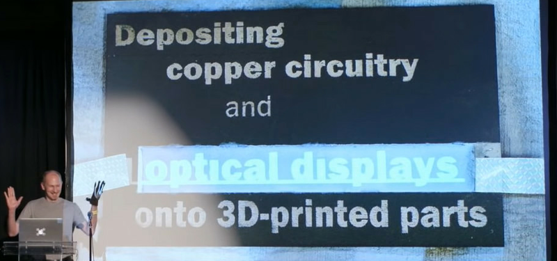
Ben Krasnow has a vision of future electronics: instead of the present PCB-screwed-into-a-plastic-box construction, flexible circuits will be deposited straight onto the plastic body of the device itself, merging the physical object and its electronics. There is existing copper-on-plastic technology, but Ben’s got something novel that he presents in this talk that you could implement yourself. You might also want a display, or at least something to blink, so he’s also working on some electroluminescent technology to complement it. If you were wondering why Ben is so interested in silkscreening photopolymers right now, watching this talk will pull a lot of interesting threads together.
Ben’s research here is truly cutting-edge. It’s prototype-able by the home gamer, but not yet production-ready for industry. Sure, there is an industrial technique for doing circuits on plastic right now. They’re not able to do plated through-holes, the plastic requires a special catalyst mixed in during injection molding, and the process requires a heavy-duty YAG laser. It’s expensive, so you could only use this process for high-margin items, and unless your garage looks different from ours, this is a non-starter for the home hacker.

Ben’s goal is to “replace the expensive parts with cheap parts”. Instead of injection molding, he wants to be able to paint the catalyst onto a 3D-printed part, and he wants to be able to draw the circuits with a sub-$100 CO2 laser. There’s a lot of great experimentation behind the results presented here, but the end result is workflow that looks like this: coat the plastic with a PTFE bike-chain lubricant to keep the catalyst from adhering. Laser the lubricant off in places where you’d like copper traces, dip the part in a wetting agent to make the catalyst stick better where the laser has gone, and then dip in catalyst and in an electroless copper plating bath. Bam!
This process is novel, affordable, and it uses some of the tools we already have access to. After watching this talk, there is nothing stopping you from getting started on this. Ben has tested this out on 2D plastic surfaces, and the main stumbling block to fully 3D plated circuits seems to be getting a 5-axis laser machine. Note that using Ben’s technique, any areas that got hit with the laser will attract copper; if you can burn holes in the substrate with the laser, you get plated through-holes for free.
As promised, Ben shifts into blinky mode for the final part of the talk. He bought some off-the-shelf electroluminescent paint, but the stuff requires some high voltage. So he designed his own driver circuitry to delivery enough juice. If you were with us in Pasadena, you surely noticed his EL glove that he was wearing around all day before his talk. And if you were in the audience, you probably sang along as he Rickrolled the entire Supercon with painted high-voltage pixels.
Since the beginning of the 3D printing revolution, we’ve all been wondering if we could 3D-print circuits, resulting in a one-shot electromechanical design process. This talk outlines one way we could get there, and makes a few compelling arguments for why you might want to join Ben on his journey. Who is going to be the first to replicate this experiment in the home lab? Or take it to the next level with a fancier laser setup?


The summary starts out making this sound so revolutionary. I was expecting printed semiconductors or something like that. Sure, printing traces is cool and all but then what? Do you quickly solder to them while risking melting the underlying plastic? Or do you attach components to the traces with carbon glue making every connection also a resistor?
Don’t get me wrong. I don’t mean to be overly negative. Every new invention is probably going to be useful to someone. I just remember going through this same thought process when it was the reprappers laying down “conductive” traces and also concluding then that this just wasn’t going to be the great new technology we were looking for.
I watched his video awhile ago, but from what I remember the plastic is fairly resistant to high temps so you can solder to it somewhat normally (the limiting factor being lifting traces due to weakening the cohesion between the deposited metal and plastic due to heat). I cant remember the specifics but he definitely does address this point in his video. I don’t know what specific application would benefit from this technique but I am absolutely sure there is something.
Cellphones you throw away.
We already have those.
They’re called “Smartphones”.
No. A smartphone is quite expensive and should have several years of lifetime with some minimal care. You must be very rich.
In my understanding a !throw awy” phone has a pricetag <=20 $.
Indeed, any mass-market technological device will achieve a point in its life where someone will call it obsolete and trash-worthy, whereas someone else will still find it useful (though not perhaps for its original purpose).
Your joke is funny, but many cellphones already have 3D-circuit antennas in them. Ironically, that’s one of the first applications of this tech industrially that Ben cited — making small, non-fragile traces that fit accurately in small spaces.
You could use lightly clamping fingers or connectors to make ZIF-like connections to these traces without significant damage.
Coated through holes would also support riveted tabs or press fit pins.
It seems to me that Ben just reads patents and then tries to recreate things described in patents. Is trying to recreate patents really that hard? Are patents really that obfuscated?
I think that historically the patent system was created as a way for inventors to share the news of their inventions widely, and thereby inspire other inventors. In that sense Ben is using the patent system exactly as designed.
Patents show the invention itself, but don’t usually don’t share the granular details of the solution. It’s not a how-to guide — that information is more like a trade secret — but describes what the general method is and the end result of it.
The United States Patent Office was created with the Patent Act of 1790. That Act was founded on these words, found in Article 1, Section 8 of the U.S. Constitution: “Congress shall have the power…to promote the progress of science and useful arts by securing for limited times to authors and inventors the exclusive right to their respective writings and discoveries.”
https://www.lexisnexisip.com/knowledge-center/the-early-history-of-the-u-s-patent-office/
The stated intent of the patent system was to protect the IP of the inventor, to allow the inventor to bring the invention to market with some protection from competitors. The fact that collectively these patents have been inspirational to others is a happy side effect.
The “promote the progress of science and the useful arts” in the Act is _exactly_ the sharing of information in question. The monopoly right was granted to entice firms to take them up on the offer, by removing the incentive to hoard trade secrets.
The idea of “IP” is a modern one — the idea that private gain should accrue to ideas (which are infinitely shareable) is a direct product of the monopoly grant. You’ve got it backwards.
If we can agree that the patent application process is essentially the disclosure of trade secrets in exchange for a chance at a temporary and exclusive right to derive profit from those trade secrets, and that the process is voluntary, then it stands to reason that inventors would only agree to this exchange if they valued the temporary monopoly over the loss of secrecy. In other words, a chance at a patent was generally a critical and required incentive for the disclosure.
The term “IP” may be new, but the core concept was very relevant, and hotly debated before, during and after the Patent Act of 1790. Thomas Jefferson was known to be opposed to patents and monopolies of any form in 1787, favoring the free exchange of ideas without regard to the original author or inventor. But by 1789, he had softened his position somewhat, and supported temporary monopolies to the original author or inventor.
https://www.monticello.org/site/research-and-collections/patents
During his time as Secretary of State (and therefore a member of the new Patent Commission) from 1790-1793, Jefferson was charged with reviewing both patent applications and the associated working demonstration model, which was a requirement at the time.
Within two months of the the passage of the Patent Act of 1790, Jefferson stated: “The patent act has given a spring to invention beyond my comprehension.”
https://www.lexisnexisip.com/knowledge-center/the-early-history-of-the-u-s-patent-office/
https://www.monticello.org/site/research-and-collections/patents
Sure, but there is no “progress of science and useful arts” without reusing and building upon the body of knowledge already discovered.
It is a trade: the power of state will uphold a monopoly to an intangible property, in exchange for the monopoly’s assured expiration and subsequent use of the said property by the public, as a common good.
Well it’s an encouragement for one to introduce that “Intangible Property” to society, otherwise it stays locked in people’s heads. A mental monopoly as it were no state can free, or public claim. Only try and create themselves under the same (dis)incentives.
This is incorrect. A patent *must* describe the invention in sufficient detail that a person of ordinary skill in the art can recreate it. If you want a patent you have to tell people how to make your invention, not just give a general description of your idea. You don’t get to combine patent protection and trade secret protection.
It seems to me that what is shown here is a *different* way to achieve the idea of the original patent. You are right that that is one of the goals of the patent system: to inspire other inventors to new inventions. I wouldn’t be at all surprised if what was described here was patentable itself – the original patent doesn’t get to claim the whole idea, just a particular way of achieving that idea.
“It seems to you”? You mean, he explicitly says in his videos that all he does is read patents and recreate them? And that he’s surprised nobody else is doing the same? I’m guessing from your belittling tone that the ‘nobody’ here also includes you?
YES…
Recreating patents can be hard, and doing so in way where you explain it to everyone else is actually really hard.
The genius here is not in reading and re-creating patents (although that can be difficult).
The genius here is in understanding them, doing low cost experimentation, then creating easy to read how-to manuals for the rest of us.
Never forget the value of someone who is REALLY GOOD at communicating technology.
Ben is genius.
Ben is a god. The single most inspiring thing that always strikes me after some binge watching of his videos is that he’s still alive and unmutilated.
Everything Ben does is extremely inspiring, A lot of people in this comment section are trying to undersell the importance of his work but the truth is that he is the only youtuber I’ve seen so far that puts this much effort into his videos.
If you still haven’t seen any of his work check him out on the Applied Science youtube channel, everything he does is top notch.
Yeah, right? I dunno who peed in their wheaties.
Seriously, though “just reads patents” is borderline offensive. He put work-weeks of work just into figuring out which catalyst/surfactant combos work best, and are yet within reach and within budget of the home gamer. This is _awesome_ work.
Plus, he’s a swell guy and is intensely good at conveying his knowledge — see YouTube or his talk. (He puts a _ton_ of work into that too…)
So yeah. Enough said. People (on the Internet) will always poop on good work. I wish they wouldn’t.
Quite right. I did email him a while back with some ideas, as my experiments with HTSCs are worthy of a post in their own right,
Regarding the novelty of this method: Laser Direct Structuring is a patented technique, for sure. However, what I describe is coating an ordinary acrylic-based polymer with oil, then ablating the oil layer with a CO2 laser, then neutralizing the surface charge left by the laser ablation with a cationic surfactant such that palladium/tin catalyst colloidal particles will stick to the laser ablated area. As far as I know, this is not described anywhere in patents or academic publications. It’s unlikely this process will rival conventional LDS for mass production. The point is to allow small shops and companies to start making these parts in prototype quantities with minimal machinery investment. This is how technology is adopted — by making it easily accessible. Also, this method is far from ready. It needs a bit more development — especially in copper adhesion to the substrate. If someone is interested in working on this, please let me know.