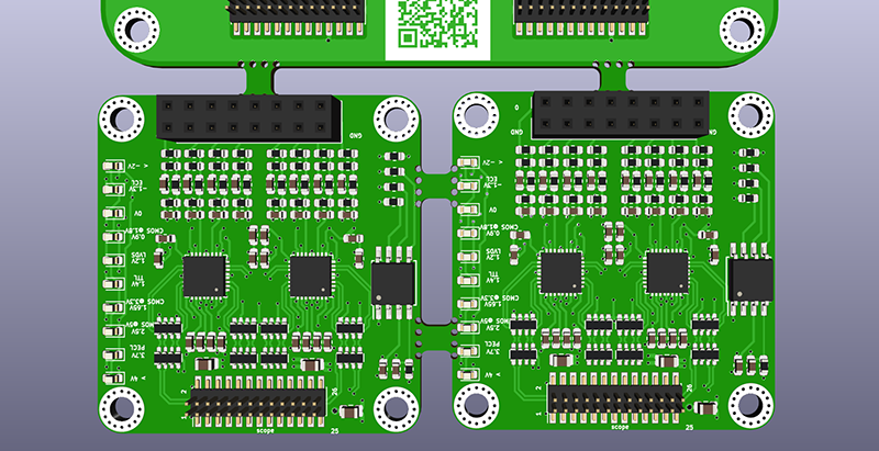
Panelization of printed circuit boards is a very helpful trick for any PCB design tool to have. By panelizing boards, you can get them ready for automated assembly. You can put testing rigs right on the panel. You can combine different boards to reduce your PCB production cost. But Eagle, Fritzing, and KiCad don’t have proper panelization tools, only hacks and third-party tools to get something close to proper panelization. [Flemming] just created a new utility for KiCad that makes multiple copies of a board connected via mouse bites. It’s not complete panelization functionality, but for a lot of us, it’ll be good enough.
The video demo for this utility (try not to click on that because we’re going to blow some bandwidth with this link) starts off by importing a board into Pcbnew, making several copies of the board, arranging these boards to have 3-4mm spacing, and drawing ‘hint lines’ for the script, telling it where the mouse bites should go. The script runs, and boom, mouse bites and a panel.
This is a KiCad specific tool, and we’ve seen other tools for KiCad that make multiple copies of a board. We’ve also seen tools that take raw Gerbers of multiple designs and turn them into a panel. [Flemming]’s efforts are the closest we’ve seen to having all the features you want out of a panelization utility bild exclusively for KiCad.
While this tool will give you a set of Gerbers with multiple copies of a board connected with mouse bites, this is not in any way a complete solution to panelizing PCBs. If you’re panelizing PCBs, you’ll want to add fiducials in the corners of the full panel, which this tool does not allow you to do. You might want to have one complete ‘frame’ as a panel — effectively a rectangular piece of fiberglass that holds all your PCBs — which this tool does not allow you to do. Since you don’t get a frame, it’s impossible to run programming or testing signals to the frame that would be needed for assembly, but not necessary in production. That said, unless you’re going to spend thousand on Altium or use Open tools that have critical flaws such as GerberPanelizer, this is the best option you’ve got.


“you’ll want to add fiducials in the corners of the full panel, which this tool does not allow you to do.”
Well, it looks like the PCB can still be edited after panelizing. So it is just a matter of drawing the fiducials manually, which is of course not ideal but easy enough.
“You might want to have one complete ‘frame’ as a panel — effectively a rectangular piece of fiberglass that holds all your PCBs — which this tool does not allow you to do.”
Looks like it’s supported looking at the readme.md? Or am I missing something?
Yeah, I added the new screenshots after the post went up on hackaday.
I tried posting a longer comment about it as well, but that seems to have gotten lost.
Doing it manually gives more control. As an eagle user I made a footprint of a mousebite and added it to my library. Making a panel takes not much time.
My basic workflow described here: https://smdprutser.nl/blog/eagle-panelizing-made-easy/
After sending the link to hackaday I implemented the bits needed for the frame, so now it’s possible to create the frame very easily, before adding the tabs.
The workflow to get frames is really as easy as it could possibly be:
* Draw two rectangles on the Edge.Cuts layer with a reasonable spacing around the existing boards to create the frames
* Adorn the frame board with registration holes and fiducials until you’re happy:)
* Add break-lines to the frame so it can be broken along with the tabs connecting the payload boards to the frame.
* Connect the new frame board to the payload boards with tabs that are solidly attached to the frame.
The two new features to enable this are:
* The ability to create a tab that stays on the frame, without a break-line.
* The ability to create a break-line in the frame itself using a line on the Eco2.User layer
https://gitlab.com/dren.dk/kicad-util/raw/master/img/panel-frame-setup.png
This results in a complete panel that looks like this:
https://gitlab.com/dren.dk/kicad-util/raw/master/img/panel-with-frame.png
The tool also has some other neat features, but more of that in another post.
Yeah sorry about that. This post sat around in the back end for two weeks.
It’s not appropriate to write about your back end Brian. :-(
Excellent work, Flemming. Thank you for a great utility!
I recently had to panelize some PCBs for production. After spending a bunch of time researching how to accomplish this in kicad I realized I could request it from my PCB supplier. Gave them the design, told them 6-UP and where to put the v-grooves. Came back perfect and my CM had no problems with it.
+1 Most people don’t realize that fab houses will panelize to your specifications for free.
Well, that’s pretty cool Flemming! Thanks for making and sharing this!
I’m currently working on my first KiCAD project. It includes multiple small boards and once it is “done” panelizing was a step I need to figure out before I submit my boards to be made.
So, anyway. I just went over to KiCAD’s site and looked at their roadmap. I was surprised to not see adding built-in panelization anywhere on their list! It seems like that feature would be an important in a modern EDA! But, anyway. Have you considered contacting them about adding that? If they agree could your new tool be integrated in as an official part of KiCAD? It might make things easier on you as you would have full access to their APIs that way. It would also mean that any future changes to KiCAD which break your tool would be considered regressions that would have to be fixed before a new release is made. That might take a lot of future maintenance work off your shoulders.
I have been thinking that putting such things into a kicad ui would be the best solution, but it’s written in C++ and writing a major piece of C++ based UI is not my idea of fun:)
The workflow is easy enough to use even if this stays as a separate utility. hopefully kicad’s pcb format/interface is stable and wont require constant “catch up” work from the author
I find this tool is pretty good for panelising any gerber files – http://blog.thisisnotrocketscience.nl/projects/pcb-panelizer/
You can also make frames and put fiducials on those too.
Thank you for this awesome & useful tool!!
Looks great but, I checked the site and downloader but what do you call, there is no ku.jar ?
Sorry, run mvn package that will produce target/kicadutil-1.0-SNAPSHOT.jar which is the jar that can be run with:
java -jar target/kicadutil-1.0-SNAPSHOT.jar I just have a shell script on my machine that runs that called ku
The file pom.xml is to do with mvn (apt-get install maven) and then having read “https://maven.apache.org/guides/getting-started/maven-in-five-minutes.html”, running the command :
mvn package, should result in a jar file being created, but I get :
WARNING: An illegal reflective access operation has occurred
WARNING: Illegal reflective access by com.google.inject.internal.cglib.core.$ReflectUtils$1 (file:/usr/share/maven/lib/guice.jar) to method java.lang.ClassLoader.defineClass(java.lang.String,byte[],int,int,java.security.ProtectionDomain)
WARNING: Please consider reporting this to the maintainers of com.google.inject.internal.cglib.core.$ReflectUtils$1
WARNING: Use –illegal-access=warn to enable warnings of further illegal reflective access operations
WARNING: All illegal access operations will be denied in a future release
[INFO] Scanning for projects…
[INFO]
[INFO] ————————————————————————
[INFO] Building kicadutil 1.0-SNAPSHOT
[INFO] ————————————————————————
[INFO]
[INFO] — maven-resources-plugin:2.6:resources (default-resources) @ kicadutil —
[WARNING] Using platform encoding (UTF-8 actually) to copy filtered resources, i.e. build is platform dependent!
[INFO] skip non existing resourceDirectory {my home dir here}/Downloads/kicad-util-master/src/main/resources
[INFO]
[INFO] — maven-compiler-plugin:3.1:compile (default-compile) @ kicadutil —
[INFO] Changes detected – recompiling the module!
[WARNING] File encoding has not been set, using platform encoding UTF-8, i.e. build is platform dependent!
[INFO] Compiling 41 source files to {my home dir here}/Downloads/kicad-util-master/target/classes
[INFO] ————————————————————-
[ERROR] COMPILATION ERROR :
[INFO] ————————————————————-
[ERROR] {my home dir here}/Downloads/kicad-util-master/src/main/java/dk/dren/kicad/layoutclone/LayoutCloner.java:[22,32] reference to Module is ambiguous
both class dk.dren.kicad.pcb.Module in dk.dren.kicad.pcb and class java.lang.Module in java.lang match
[INFO] 1 error
[INFO] ————————————————————-
[INFO] ————————————————————————
[INFO] BUILD FAILURE
[INFO] ————————————————————————
[INFO] Total time: 2.794 s
[INFO] Finished at: 2019-03-26T14:36:28Z
[INFO] Final Memory: 15M/54M
[INFO] ————————————————————————
[ERROR] Failed to execute goal org.apache.maven.plugins:maven-compiler-plugin:3.1:compile (default-compile) on project kicadutil: Compilation failure
[ERROR] {my home dir here}/Downloads/kicad-util-master/src/main/java/dk/dren/kicad/layoutclone/LayoutCloner.java:[22,32] reference to Module is ambiguous
[ERROR] both class dk.dren.kicad.pcb.Module in dk.dren.kicad.pcb and class java.lang.Module in java.lang match
[ERROR]
[ERROR] -> [Help 1]
[ERROR]
[ERROR] To see the full stack trace of the errors, re-run Maven with the -e switch.
[ERROR] Re-run Maven using the -X switch to enable full debug logging.
[ERROR]
[ERROR] For more information about the errors and possible solutions, please read the following articles:
[ERROR] [Help 1] http://cwiki.apache.org/confluence/display/MAVEN/MojoFailureException
Any ideas Author or java people ?
Thanks
Hmm, can you try with JDK 8 ?
Thanks, will do, (just accepted the default jre first time around).
Hi Flemming, was using mint 19.1, with default-jre/jdk changed to openjdk-8 and now I’ve got the jar file !
Thanks for your help.
Now getting :
java -jar ku.jar pcb -f=noname.kicad_pcb panel
picocli.CommandLine$ExecutionException: Error while calling command (dk.dren.kicad.cmd.PanelStitching@59a6e353): java.lang.IllegalArgumentException: Could not find an edge cut line that intersects the Eco1.User line from Point(x=205.105000, y=127.571500) to Point(x=205.105000, y=132.080000)
at picocli.CommandLine.execute(CommandLine.java:1180)
at picocli.CommandLine.access$800(CommandLine.java:141)
at picocli.CommandLine$RunAll.handle(CommandLine.java:1416)
at picocli.CommandLine$RunAll.handle(CommandLine.java:1376)
at picocli.CommandLine$AbstractParseResultHandler.handleParseResult(CommandLine.java:1243)
at picocli.CommandLine.parseWithHandlers(CommandLine.java:1526)
at dk.dren.kicad.cmd.Main.main(Main.java:33)
Caused by: java.lang.IllegalArgumentException: Could not find an edge cut line that intersects the Eco1.User line from Point(x=205.105000, y=127.571500) to Point(x=205.105000, y=132.080000)
at dk.dren.kicad.cmd.PanelStitching.halfStitch(PanelStitching.java:161)
at dk.dren.kicad.cmd.PanelStitching.call(PanelStitching.java:79)
at dk.dren.kicad.cmd.PanelStitching.call(PanelStitching.java:17)
at picocli.CommandLine.execute(CommandLine.java:1173)
… 6 more
Which is strange because for testing I’m only using a single line on Eco1.User and it really is intersecting both PCB’s !
Is there any reason why it wouldn’t work (my pcb’s that have curved corners ?) I’m connecting the 2 PCB’s on a straight edge away from the corners.
I am also having same issue. No idea what is fix.
I have tried with round as well as square but still having same result.
Finally I got it working with square boarder PCBs. Great Work Flemming !
Somehow this script is not working with Round Shape PCBs. — Any solution for that?
Great tool! Using kicad-util I have panelized Adafruit’s SMT break-out boards:
https://www.jsykora.info/2019/06/pcb-panel-of-smt-breakout-boards-soic-tssop-msop/
I would wish this tool or similar was integrated in Pcbnew. Thanks!
Is this working on kicad 5.1.2? I have a very simple 4 board layout with Eco1.User lines crossing Edge.Cuts lines and when I try to run the ‘panel’ command, it looks like it has done something but the kicad_pcb file has not been changed.
❯ java -jar /Users/ilium007/Downloads/kicadutil.jar pcb –file=/Users/ilium007/Documents/KiCad/test_project/noname.kicad_pcb panel