If you play with high speed design for long enough, eventually you’re going to run into clock skew and other weird effects. [Robert Feranec] recently ran into this problem and found an interesting solution to visualizing electric fields in a PCB.
A word of warning before we dig into this, for most of the projects we see on Hackaday something like this is completely superfluous. There aren’t many people dealing with high speed interfaces here, and there aren’t many people dealing with 100 Gigabit per second data links, period. That said, it’s not unheard of, and at the very least it’s interesting to look at.
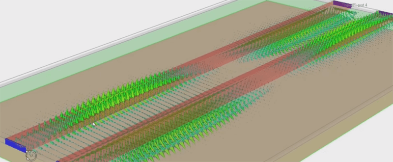
The basics of this video is simulating the signals visually in a differential pair on a (virtual) printed circuit board. The software for this is Simbeor, and [Robert] talked to the founder of the company behind this software after watching a video on simulating electric fields in differential traces. This software does what it says, and is a great illustration of why differential pairs must have the same length.
While this might not be for everyone, it is a fantastic visualization of signals in high-speed design that goes above and beyond what you would expect from a Spice simulation. Even if you’re not doing high-speed design, you may someday and it’s never too soon to get an intuitive understanding of how electrons work.


Useful. Good to see Hackaday is interested in more than blinkies!
Modern logic requires signal integrity. SI was becoming a problem in the 80s, and hasn’t got better since then. If you don’t have good SI, then the receiver will not be able to correctly interpret the *analogue* input[1] as a digital signal – and you will end up with intermittent or rare failures.
[1] the only digital circuits are femtoamp circuits and photon counting circuits. Yes, that is a slight exaggeration, to make the point.
Agreed, now I can finally build my own 100Gbe card! (ha). Interesting stuff though, the amount of knowledge you need to be able to reasonably work with some of the crazy high data rates. I know that was an exaggeration above, but pushing 100G over an LC connection, counting photons doesn’t seem to far off…. Some of these small 32port switches that can backplane over 6Tb/s seem like they would take some ‘extreme engineering’.
Honestly it feels like an ads…. Why not mentioning other software if it’s not, some of them even useful for the hobbyist because they have cool license ?!
In commercial one, Sonnet offers a free license with enough feature to do basic tests. There are FEKO, HFSS, and many other ones…
In Free software…. there are ton of them !
OpenEMS, Elmer, EMGine, SparseLizard and so many more…
Seriously, you could at least publish the list, it’s better than shamelessly cross post youtube video of a really expensive piece of software…
Thanks for all the free ones :)
I recently downloaded CST Studio Suite 2018 Student Edition and haven’t gotten to work with yet. https://www.cst.com/academia/student-edition/download
There are some other simulation software that I was wanting to look into more for the microstrip, stripline, finline and all sorts of other thin or thick or whatever slot or other line.
I forget at the moment that I was reading about that seemed interesting for microwave work.
“for most of the projects we see on Hackaday something like this is completely superfluous” Um…maybe. if you are doing the layout for a switching power supply this could be a valueable tool.
I didn’t think you’d even be into the megahertz with a SMPSU … or are you designing on a square kilometer of board?
Harmonics.
Many modern switching converters have switching frequencies of up to a few MHz.
It’s not about the frequency it’s about total signal spectrum i.e. rising / falling time. You could have SI problems with only 1kHz square signal if you have very sharp edges.
That software is amazing! I’ve always wondered how these signals really travel on complex boards and this thing actually shows you what goes on. Nice.
We haven’t tried this yet – would be cool to do a demo of this software with our next design and see if/how it helps us! We do a lot of high speed layout over at PCBLayout.com, and this would be a really useful tool. Awesome, thanks!
This is probably a better solution than the Matlab programs I’ve written to attempt similar things.
I think the net result is that PC board traces have to be considered as RF transmission lines, complete with characteristic impedances, and impedance matching. Additionally, since the speed of propagation of the signal depends upon the permittivity and permeability of the surrounding insulating medium, these have to be factored in. However, since the conductors are, for the most part, in a inhomogeneous medium (where part of the insulation is composed of fiberglass or other insulator, while the other part is composed of air, at least for non-multi-layer boards), you can get some weird pulse smearing effects. Of course, given the fact that the geometry of the traces on the PC board are usually rectangles, this makes finding the per unit length capacitance and inductance difficult, if not impossible (Try solving Maxwell’s Equations for these shapes.). Then, when you realize that you have multiple conductors, the equations become matrices, and you end up with characteristic impedances from each conductor to every other conductor. This will make your head hurt, especially when you start considering the SWR vectors, and crosstalk from one line to another. And, if you really want to make your head explode, consider that the permittivity of the dielectric very well may be frequency dependent.
If you’ll pardon a shameless plug, the book “Analysis of Multiconductor Transmission LInes”, by Dr. Clayton R. Paul, is one of the better books on the subject. I studied under the late Dr. Paul while he was literally writing that book, as a graduate level course in EE, back in the mid-1980s.
That software is amazing! I’ve always wondered how these signals really travel on complex boards and this thing actually shows you what goes on. Nice.