By now we are all used to the role of the printed circuit board in artwork, because of the burgeoning creativity in the conference and unofficial #BadgeLife electronic badge scenes. When the masters of electronic design tools turn their hand to producing for aesthetic rather than technical reasons, the results were always going to be something rather special.
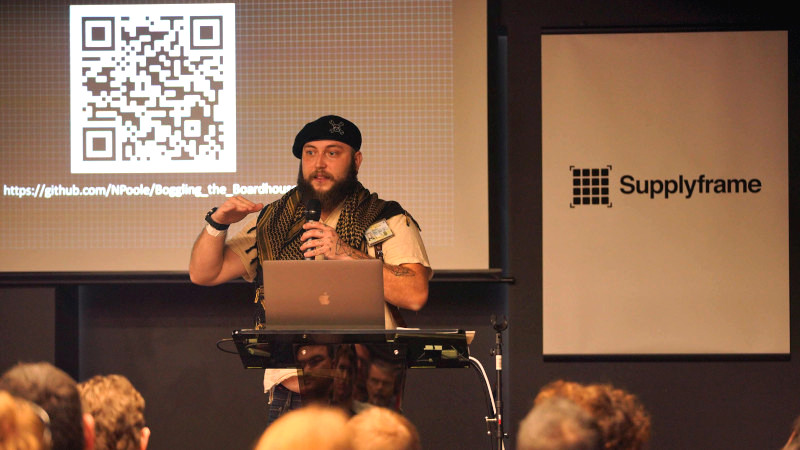
Nick Poole is an ace wrangler of electrons working for SparkFun, and as such is someone with an impressive pedigree when it comes to PCB design. Coming on stage sporting a beret with an awesome cap badge, his talk at the recent Hackaday Superconference concerned his experience in pushing the boundaries of what is possible in PCB manufacture. It was a primer in the techniques required to create special work in the medium of printed circuit boards, and it should be essential viewing for anybody with an interest in this field.
Though he starts with the basics of importing graphics into a PCB design package, the meat of his talk lies in going beyond the mere two dimensions of a single PCB into the third dimension either by creating PCBs that interlock, or by stacking boards.
As an example anyone who has ever soldered two PCBs together at right angles will know the pain of lifting an area of copper as the heat delaminates the PCB. His tip of placing vias to anchor the layers is typical of the kind of expert knowledge contained in the talk.
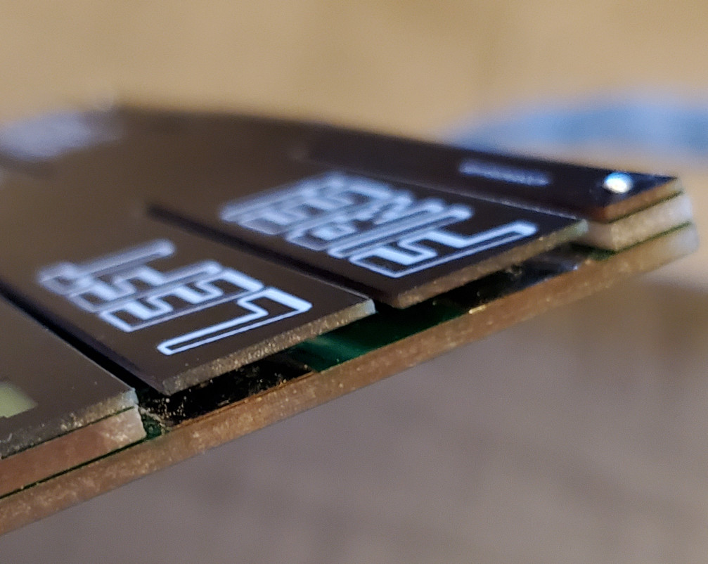 Continuing on through mouse bites, translucent displays, and switches using the springiness of PCB fingers, he uses his space invader badge as an example. This badge sports three layers and an array of APA102 addressable LEDs shining through a milled-out middle layer and a translucent top layer. Along the way we learn yet more valuable tips. Putting notes for the board house technicians as text in the off-board parts of layers that make it to the Gerbers helps immensely when boundaries are being pushed, as often the staff will question something that departs significantly from their norm.
Whether it is conquering the inside corner problem, ensuring crenelations for plated edges, or joining multiple boards together in a stack, we think there should be plenty here to keep you occupied as you take your PCB work to the next level.


I want a Jolly Wrencher beret!
Do what Nick did! Stick a Jolly Wrencher on your beret. :)
No, I want someone else to do it for me.
B^)
Great talk with many useful tools to keep in the pcb design toolbox. I used many of the ideas presented to make my small pcb word clock and was surprised how clean and professionally it came out.
He sounds fine to me. The only thing cringeworthy is usage of the word cringe anymore.
Cringeworthy in what way?
Viva la resistor … erm I mean resistance?
I’m dubious about how often this is useful, but it looks cool: a coworker would always put a soldermask cutout on the top and bottom layers, and then put a number in copper on each internal layer in the window the soldermask cutout provided, so he could hold the board up to a bright light and visually verify all the internal layers and the stackup order when he got the board back from fab.
Whoa, I like that! I’m also not sure how often that’s a problem worth inspecting for but it’s a cool method of inspection.