[SaltyPuglord] needed a solid state relay for a project. We’d have just bought one, but he decided to design his own in LTSpice. Along the way he made the video below, which is pretty informative and a good example of a non-trivial design in LTSpice.
MOSFETs have made designs like this a lot easier, to the extent that it should be as easy as putting a pair of beefy fets in-line with the AC source and load. However, that has a few ramifications that [Salty] covers in the video.
The biggest concern comes in isolating the DC supply from ground. He used a transformer which is tricky to simulate in LTSpice. Beyond that the design of the power supply is quite simple, and as he mentions in the video, you don’t really need this complex of a regulator just to feed the gates of the MOSFETs.
The other issue is that the wires between the two MOSFETS really have to float and could handle quite a bit of current. The problem is, LTSpice can become confused if there’s no ground reference for the FETs. Thus there is a ground in the simulated circuit. In fact, the default LTSpice solver doesn’t like the circuit anyway. The video shows how to change to the alternative solver which works well.
It looks as though a lot of what the video talks about is also mentioned in a linked document from TI. If you want to try a light version of the circuit without installing LTSpice, try Falstad. Or try Micro Cap if you want to install something different. If you do stick with LTSpice and you want to learn more about modeling transformers, we’ve got you covered.


This has to be the most complicated solid state relay I have seen to date. Does he explain why he takes such a circuitous route? All you need is an optocoupler and a SCR, maybe some snubber components if you are feeling adventurous. You can even get opto isolators with zero crossing detection integrated if that is important to you.
ex http://bristolwatch.com/ele/triacs2.htm
the advantage of mosfets is that you can turn off instantly at any time so with current sense you can make it short circuit proof
SCR/TRIAC SSR’s dissipate like a B*#CH at higher currents, a MOSFET approach is a significant improvement.
In the scheme he proposes one of the mosfets is reverse biased, so you will have roughly the same voltage drop as a SCR across the reverse biased device, not to mention the voltage drop across the forward biased device. At 10A RMS the mosfets he used will drop about 4v across the ‘on’ device at 25C case temperature (increasing with temperature to 6v at 150C case temperature) and another 1v across the ‘off’ device, for a total of about 50w of power dissipation (increasing 70w at 150C case temperature).
Consider instead the similarly priced triac [1] which only has a single diode drop of about 1v at 10amps. This device will dissipate less than 10W at the same 10A RMS current, and is much simpler to power (no extra power supply or gate drive needed). Note that the voltage drop across a SCR actually decreases slightly with increasing temperature, so power dissipation actually improves slightly with increasing case temperature.
[1] https://www.digikey.com/product-detail/en/littelfuse-inc/Q6035NH5TP/Q6035NH5TP-ND/967581
Or consider this triac [2] which costs 1/10 as much as the mosfet, but can handle the same current and will dissipate about 15w max, roughly 1/5 as much as the mosfet design.
[2] https://www.digikey.com/product-detail/en/rochester-electronics-llc/MAC12M/2156-MAC12M-ON-ND/11522873
It is certainly possible to design a mosfet based approach which will outperform a triac based device, but for line voltage applications it is horrendously expensive. It really only makes sense for DC or low voltage applications where you can find mosfets with ESR of a few milliohms.
the mosfets are only reverse biased when off, when they are on they conduct in both direction so the only limit is how low an on resistance you can get.
At 10A the voltage drop across the internal body diode is less than 1v, where as the voltage drop across the main mosfet is >4v, so the current is going to flow through the body diode in the reverse biased device.
You are correct that in a well designed SSR you could avoid this, but this is only true in the authors design for currents under 1amp.
If he wanted to compete with a triac at 10A of current he would need mosfets with under 50mR on resistance, which are about >$10 a piece compared to $0.23 for the triac based solution.
you are right, I wrongly assumed he had made a sensible choice of mosfet. The advantage of using mosfets is that they can turn off instantly, not limited to the end of a cycle. I’ve used it to make an electronic fuse in front of a number off triacs so they wouldn’t grenade in case of a short
Check again – ain’t no diodes when those fets are on! (and ain’t no diodes when those fets are off.) Diode drops were if there was a current path yet if fets have fully biased Gate-Source a good fet for this would have about 38mOhms and when open both diodes are back to back so no conduction path. Look again.
Btw whether Triac, Relay or FET you want a circuit breaker or fuse beyond target use.
I wonder why he doesn’t take the gate voltage dircetly from mains with a couple of caps and diodes instead of using a clumsy transformer. The only current you need would be the miniscule current flowing through the gates’ pull-down resistor.
Unless the AC mains for biasing is isolated from the circuit you are switching, there is a chance that you could short circuit between that and the switched circuit by user error.
Real life MOSFET based SSR uses LED emitter with small photovoltaic cells to drive the MOSFET gates. They might also be used to power the optional zero crossing detection circuit for AC units.
It is a lot easier for TRIAC based designs because you can use the voltage across the device as the trigger source. Once it is triggered, it stays on until the next zero crossing.
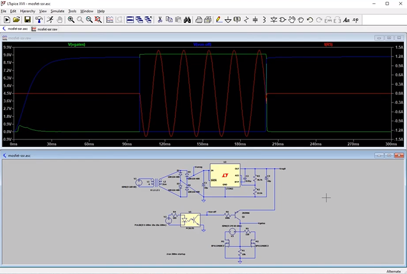
So… is it R1 or R5 that represents the load being switched?
And if one was to actually build this circuit would they omit said resistor in place of the load? Or keep it in to provide a minimum load?
R5 is the load, R1 is a pull down for the gates
sad not work with DC current like mechanical relay, high power DC loads or untouched bidirectional DC signals keep SSRs out almost all my projects. Oh and zero-crossing its not a feature for me its an issue, when i need shut down i need shut down immediately not when the device whants.