Around these parts we tend to be exponents of the KiCad lifestyle; what better way to design a PCBA than with free and open source tools that run anywhere? But there are still capabilities in commercial EDA packages that haven’t found their way into KiCad yet, so it may not always be the best tool for the job. Altium Designer is a popular non-libre option, but at up to tens of thousands of USD per seat it’s not always a good fit for users and businesses without a serious need.
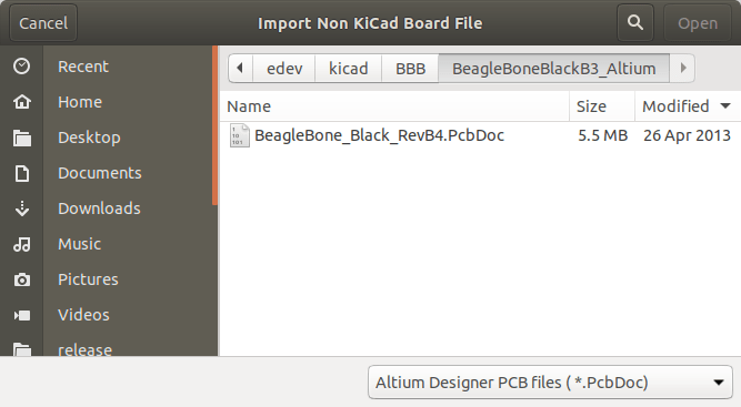
What do you do as a KiCad user who encounters a design in Altium you’d like to work with? Well as of April 3rd 2020, [Thomas Pointhuber] has merged the beginnings of a native Altium importer into KiCad which looks to be slated for the 6.0 release. As [Thomas] himself points out in the patch submission, this is hardly the first time a 3rd party Altium importer has been published. His new work is a translation of the Perl plugin altium2kicad by [thesourcerer8]. And back in January another user left a comment with links to four other (non-KiCad) tools to handle Altium files.
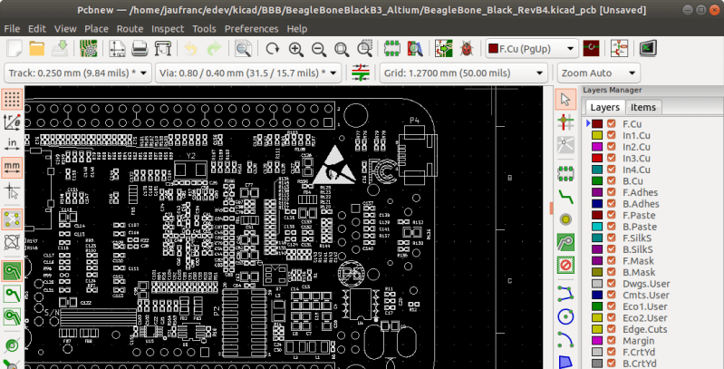
If you’d like to try out this nifty new feature for yourself, CNX has a great walkthrough starting at building KiCad from source. As for documents to test against the classic BeagleBone Black sources seen above can be found at on GitHub. Head past the break to check out the very boring, but very exciting video of the importer at work, courtesy of [Thomas] himself. We can’t wait to give this a shot!
Thanks for the tip [Chris Gammell]!
Finally, importing #altium boards into #kicad is only one click away (in the developer version).
This allows to view and edit #opensource #hardware which was designed with #proprietary software, and thus, in fact, not open for everyone. pic.twitter.com/oogiJeyynW
— Thomas Pointhuber (@Chaos_Robotic) April 4, 2020


I’m a huge Altium fan, so I like to suggest CircuitMaker as a free alternative. It’s basically a dumbed down version of Altium, but still has great features. It’s my current go-to software for personal pcb projects.
Well, if someone wants to import your project it into KiCad, my importer also supports CircuitMaker and CircuitStudio.
“we tend to be exponents of the KiCad lifestyle;” was that intentional? (exponents)
Opponents oppose the pone, proponents support the pone, exponents spray the pone everywhere.
ya know altium has a free version …
But it’s not open source, so by default it is pure evil and must be shunned. And most importantly it wont even run on your Linux install from 1996 that you run on your old converted Amiga so what good is it anyway.
Hahhahah!! That was good!
The only good pcb designs are on vinyl.
It hasn’t been updated in years, and was pretty beta even before it was abandoned. It’s unfortunate, I liked it a lot.
In response to your comment of Altium costs …” but at up to tens of thousands of USD per seat” … This may be the retail or listed price, but from time to time Altium has special offers (like the Spring of 2019) and one could have a full perpetual Altium seat for less than $3K USD (including access to online training and a year of support). Although $3K is not inexpensive it is certainly reasonable for many smaller to medium sized companies.
The small company I work at has under 50 employees, and 10 of them do electronics design… How could we justify waiting for a “sale” to upgrade the department seats? Between our old OrCAD, Eagle, and Altium seats, we are now in process of moving everyone to KiCAD. Some people are looking at what’s in the development for 6.0 and are excited for a number of features. We are looking at what are some of the things we need that aren’t being developed and are making a business case for assigning a developer to do part-time coding on kicad within our company – with it being released as open source as it’s worked on. Open source is the way of the future.
Wayne Stambaugh an Seth Hillbrand ( 2 mayor KiCad developers) have setup https://www.kipro-pcb.com for commercial support. They can help with getting your own developers up to speed, or you can hire them for some custom work on KiCad.
Thank you, I’ll look into that!
As a hobbyist who uses kicad, and not any of the paid alternatives, what features am I missing?
Apparently a very expensive seat :)
Altium makes it much more comfortable to sit in that seat due to a much thinner wallet.
as a hobbyist? Probably nothing. Unless you are doing very complex boards!
8 years ago we made the switch from Kicad to Altium, primarly because it allows to succeed complex boards easily compared to Kicad.
One of the best features I think Altium has is the very refined Design Rules. You can pretty much say “I want my 10Ohms diff pairs to be 0.22mm wide on Top layer, 0.174mm on layer 3, but 0.1mm is fine under this fine pitch BGA” , or “I want normal clearance to be 0.125mm, but between polygon pour and trace it’s 0.15mm. Oh, and I want to have 2mm clearance between my AC input and the rest of the circuit”
These rules would be used automatically when pouring polygons, and (most of times) when routing traces.
In most designs we have at least 20 rules. It clears the most common routing mistakes you could do. Especially useful when working with others on high-speed design or if there are specific safety-related clearances to respect, where sometimes a simple mistake as a misplaced trace would mean a costly and expensive respin (much much more costly than an Altium Licence).
And finally, there are so many “smart routing” tools that once mastered enables you to go 2-10x faster than manual. Plus the ability to use STEP 3D models so you can get an accurate final 3D model for mechanical integration. Plus the 1000 little things like muti-channed design (copy-paste your routing in seconds).
There are some downsides though. it’s a tool that takes a lot of learning and practice to use at its full potential, and it might not be worth it “just for one board from time to time”.
TBH, now that Kicad has made lots of progress on the routing part, I’m tempted to go back to it though. First for personal projects, then maybe for professional ones (but we’d have to add Design Rules to it though).
One of the reasons being that in Kicad every files are text-based, which play (relatively) nice with Git and allow to build some verification tools around it. It’s a bit easier than reverse-engineering the partly-text-partly-binary-collage-of-partially-duplicated-information-shoved-in-an-OLE that Altium files are. Thomas Pointhuber most likely know that even better than I do :)
tl; dr
As a summary, I’d say that Altium is better than Kicad if
– your design is 1000 components or more
– your design has complex clearance or mechanical constrains (or ultra-fine pitch)
– your design will be used in an “high exigence” industry
– you make a lot of revisions of lots of boards
So, as a hobbyist you could fall into one of these categories, but it’s unlikely.
1+
Probably the most accurate comparison. I’ve recently started using kicad again (tried it in 2015 and wasn’t impressed), the libraries AND integrated 3d models are absolutely incredible. I can do a ray traced 3d model of the complete board (pretty pictures) and export the 3d board and component models for mechanical integration. If PCB design is your daily job id stick with altium :)
Fun fact: KiCad is better than Altium if you have more than 65534 components or nets, simply because the file format uses 16 bit (I hope unsigned) integers. It cannot represent more.
For the constraints: I did not implemented them yet, simply because KiCad 6 will get a system very similar to Altium.
Indeed, there will be a new cool constraint system. PS. I don’t know what hardware @chmousset runs Altium on, but in my experience one ~1500-pin BGA + a few memories make Altium unusably sluggish.
I mostly work on high-end laptop with dedicated GPU. In the past, GPU seemed to be the bottleneck (maybe not in FHD; but was the case for me in 4k) but since AD19 it seems to be more of a CPU-hog. The biggest design I have is 1000 component, 22k pads, about 40 planes and yes, it does run pretty sluggish when multi-routing 20 nets (even when zooming I get ~20FPS). There are some tweaks that seems to be useful in online DRC but haven’t figured out a way to get everything *really* smooth.
I’m not too sure Altium could handle 10k components at all TBH. I don’t think the 16bits file format is where the practical limit is :)
In comparison the same design imported in pcbnew renders silky smooth. But polygon generation is 100x slower than Altium and ultimately crashed pcbnew…
8 years ago we made the switch from Kicad to Altium
Eight years is a very long time for a fast-developed program like KiCAD! I have never used Altium, but I think that KiCAD is developed at a much faster rate than Altium. Also, see my response to Alexander Wikström below. KiCAD has a whole echosystem of pugins built around it and has been “married” to FreeCAD, an open-source mechanical CAD, greatly easing 3D work. You can push-pull mechanical stuff (incl. STEP data) between the two very easily.
>Eight years is a very long time for a fast-developed program like KiCAD!
Which is exactly why I can consider moving back to it for personal projects and maybe even professional ones ;)
Every ‘big’ professional software (Altium, Solidworks, Catia at its time) eventually reach a point where reverse-compatibility and maintaining the user’s workflow as stable as possible prevent them from adding new features, or do things smarter.
In the Solidworks case, that I’ve been using for maybe 15 years, very little improvements happened from say the 2010 and the 2016 versions (at least for my rather ‘basic’ usage). Then Fusion 360 came and changed everything for me. I’m probably 2-3x more efficient, and it comes with free FEM, for a fraction of the price. Indeed, Fusion will also reach a point of standstill in the future, but it’s still far (20-30 years cycle). Kicad will probably know it too. :)
> KiCAD has a whole echosystem of pugins built around it and has been “married” to FreeCAD
I don’t want FreeCAD. I want the step (pun intended) of exporting the PCB 3D model as simple as possible, so I can put that model into the MCAD package I prefer. But that’s my liking.
I dunno. Methinks most ‘big’ companies are apt to use mentor and/or cadence.
And the big difference for me is that KiCad runs on Linux, and the power of Python scripts for DRC and lib management. But there is much other interesting stuff – such as Sourcery CodeBench from mentor.
For the person doing the board layout, the differences are most notable in the component libraries and component editing features.
Python ? DRC? You have my attention :)
Do you have any example in mind?
I do use KiCAD myself. But when one can go make a long list of annoying quirks that KiCAD does, then it isn’t really an all that good piece of software.
Thankfully some minor details can be altered with settings. But some quirks seems to be intentional.
Eeschema’s ineptitude at doing basic selection of objects is down right frustrating. (Selecting doesn’t = moving…. And selecting multiple items by holding down a key and clicking each item one wants would also be a nice improvement. (Since nearly every CAD program in existence seems to support this…))
Editing properties of multiple components would also be a nice thing to have. I can understand component references not being “supported” (even if this too could be made in a logical fashion.), but it would be nice if I could set that footprint on the components. Or maybe even add a “reference” so that the component just follows whatever I set the reference too. Same thing goes for linking in datasheets and whatever else one might need.
Deleting lines in Eeschema is also annoying to say the least. Why does it have to delete the whole line? Can’t it stop at an junction? (Yes, I can go and redraw that part, but I shouldn’t have too.)
We also have the component library that is full of nearly everything one needs, and it isn’t all that hard to add new stuff to it.
But creating new library components could be a heck of a lot easier and primarily quicker… Nearly all components one makes will be a rectangular box. With a bunch of pins on X sides of it… Why can’t it generate this for us? All it needs to know is how many pins we have, what the component is called, what the pins are called and what the pins do. (if we want to have basic debugging later.)
Then we have the footprint library.
Other then the footprint library crashing at times, it isn’t all that bad.
The library contains multiple copies of some components though. What is the difference between a 0805 Capacitor and an 0805 resistor? And why does the 0805 Inductor, diode, etc need their own footprints? Can’t we just have one library for all 1206, 0805, 0603, 0201, etc, etc footprints. They are supposed to be identical after all…. (They are frankly so standardized that we could generate them when needed, saving us the need of having to have hundreds of files for them…)
KiCad already has a generator for both BGA’s (not seeming to support staggered pins), SOIC, S-DIP (nostaggered pins), QFP, FPC. So this is nice. Now if only we could have a standard way to tell the program to auto generate a footprint. Instead of the current need to first generate it, put it into a library (or make a new library for it) and then point the component at that footprint…
How hard could it be to just tell the program, “generate:BGA,5×5,pp-.5,ps-.3,mx-.5,my-.5” and have it generate a 5 by 5 pin BGA with a pad size of 0.3 mm, pad pitch of 0.5 mm and an outline of 0.5 mm. Now I don’t advocate for my just made up way of formatting, but it would be nice to say that one wants to generate a new footprint instead of always needing a library for everything. Would also make the project more portable. Since all one would need is the generator and not have to fiddle with importing libraries.
Downside is if a chip has missing pins (or just staggered pins at the moment…). Some BGAs after all have a + sign of missing pins, some have whole squares missing, or other patterns. Some chips might even toss in a far larger pad. But for the real odd chips, that is where a library becomes immensely useful.
But kicad of cores have a bizzilion other problems strewn out all over the place. Don’t know if the latest version of PCBnew still always have the “auto delete old track” function active regardless of what the button in the UI is set to….
PCBnew also has this wonderful little issue when using the DRC tool. It does make a long list of all problems, even marks them with arrows. But there is no ID’s on the arrows, nor any ID on the problem. Would be wonderful if problem 1 first of had a #1 besides it, and the corresponding arrow also had a #1 besides it too…. Not to mention when clicking the arrow that it also lights up the offending trace(s), via(s), or component(s). (Just like it lights up the corresponding pads/tracks when one draws the traces.)
Would also be nice if:
1. one could add a text document or three to one’s project… For project documentation.
2. Kicad supported version history of one’s project. So that if one wants to make an alteration, one can insert a “bookmark” for that point in time, and then fiddle about making the alteration. While still always having the option to go back to the prior version. This means that we can worry less about redesigning parts, since we know that the prior version still is there. (Yes, we should be able to have multiple bookmarks. Some CAD programs saves every little thing one does as a “history”, but this is overly detailed and just makes it harder to actually know where one came from, and for going back shorter distances, “undo”/ctrl-Z is more effective.) Simplest implementation is to be able to have multiple versions of that PCB file in the project.
3. we could have multiple different boards for the same project. Ie, each board would likely have its own schematics. And the ability to import these boards into each other and have them sit where they should when using the 3D viewer. For the more complicated 3D designs. So if the schematics states that two boards are connected, then they get connected in the 3D viewer. (Though, I can also see how a simple mistake in the code could lead to the program making endless recursion when having for an example having 4 interconnected boards making a cube… Not to mention how flex PCBs would be handled… (but flex PCBs is another topic all together…))
4. we could export the 3D models from kicad to stuff into other CAD programs where we make other parts of the same project….. Fit to envelope design would suddenly be a lot easier. (The 3D viewer can export an image at current, but nothing else…)
5. we could have a Bill of Materials file as part of the project, so that we know how many components we need and of what type. Preferably with support for the aforementioned version history. Maybe even be able to take notes inside of it, maybe even doing inventory checking through Octopart or the like.
But this comment is now a text wall, so I’ll end it here.
Every EDA tool has annoying quirks. Just because you’re used to the quirks of doesn’t mean it’s perfect.
Ugh, “Just because you’re used to the quirks of [insert preferred EDA tool here] doesn’t mean it’s perfect”.
I don’t think any CAD tool is perfect to be fair.
They all have their downsides, even a feature rich tool can fall flat on its face in some cases.
But do note how non of my complains have been that KiCAD should behave/work like another program.
I have stated that it does stuff that frankly isn’t logical if one wants to expand the programs capabilities.
For an example, KiCAD’s desire to always move what one has selected, is a thing that the program needs to change if it wants to support the ability to change specifications on multiple components in parallel.
The desire to organize and clean up the footprint library and generally give it a wider range of features (ie native foot print generation) is a thing that would allow KiCAD to do even more things, while still retaining all the current ways of using the program.
Then there is of cores those features that doesn’t even do what they state on the tin… That is objectively a problem that needs to be fixed.
My goal isn’t to make KiCAD act like Eagle, or Altium, or any other PCB CAD program.
Not to mention that a third of my comment isn’t even complaining about problems, but rather suggesting new features to expand on the programs capabilities and make it useful for a wider audience, while aiming at having a fairly minor impact on how current users use the program.
Sometimes one can’t though add new features if another feature makes it hard to implement.
Like selecting stuff shouldn’t move the stuff around. While another thing like deleting a line brings up the question if we should delete the whole line or just to nearest junctions. This should generally be a user setting. (or even switched on the fly using a key like shift)
In the end, KiCAD isn’t inherently bad. It is though riddled with minor bugs that can make it a fairly horrid experience at times. Not to mention when it crashes. (thankfully fairly rare.)
GIMP is another program that is a bit like KiCAD, but for photoediting/drawing. It too is riddled with bugs, have some quirky features, and generally does things a bit oddly at times. Does that mean it is inherently bad and should instead behave like Photoshop? No, not really.
But both GIMP and KiCAD should aim at supporting a wide verity of workflows, mainly because there is a wide verity of people using said programs, for widely different things.
So the idea that “I am used to [insert preferred CAD tool here], therefor KiCAD should behave like that!” is frankly the complete opposite of what I aim for.
Multiple 0805 library symbols exist at least because they have different 3D footprints attached. Resistors, capacitors, diodes, LED’s all look different on the 3D view.
The Footprint generation wizards in KiCad are short python scripts. Usually 200 lines or so. So if you want to make a custom footprint wizard for some as yet unsupported footprint you have nice examples to start from.
I agree though that Eeschema has been left behind a bit. Most of the development for KiCad V5 went into Pcbnew. Eeschema is not left behind for KiCad V6 though, and will get some mayor updates. That may still be a year or so before a stable version is released though.
Because of it’s open-ness KiCad also supports a big and growing amount of extensions and related projects. For a different workflow, take skidl for example. It’s a python library which can generate net lists and more from scripts. It’s a bit like VHDL for PCB design.
I’m a daily user of Altium. By no means is it perfect – the idea is laughable.
_kicad is worse._
It’s just the plain facts. Every time I discover a new infuriating aspect of Altium, every time I wish I could throw my computer off a cliff I reflect on whether I could have done it better in Kicad. And the answer has always been no.
You can export a 3D model from KiCAD as a STEP or VRML file… It’s just in the main menu, under File > Export, not in the 3D viewer.
Well, not where I would expect to find it. But that works too. Now it would be nice if it supported more files. But that is a minor issue.
You can delete a simple line segment in eeschema, just click on that segment and press DEL button.
To be honest I was using Altium for decades (since 98) and there are so many bugs and the most annoying and serious(needs complete restart) ones (like dll exceptions due to drc or parameter parsing error, or dll exceptions for whatever random occasions) – are still there. They can’t fix in 20 years. And there are a tons of simply annoying bugs in PCB editor. There aren’t perfect EDA.
Btw. you have to re-learn the shortcuts, operations and you will find out KiCAD can do almost everything what you use often in Altium.
1. You can add text to your project. Simply create a txt file in project dir and you will see it in the list. When you open it you can choose editor program for that file.
2. Since KiCAD files are text based you can use SVN, GIT or whatever you like for versioning.
3. Yes it is missing now…
4. You can export it. Pcbnew: File->Export->STEP
5. BOM versioning could be done via GIT or SVN too, but yes, sophisticated variant management is missing.
I myself have looked at people using Altium, and long since made the decision to not touch it. It really doesn’t seem to have that many advantages over KiCAD. At least nothing worth the frankly insane costs it carries.
In version 4.0.7 at least is doesn’t delete things in a nice fashion. Might have changed that in the current 5.1.4 version. But it frankly wouldn’t surprise me if it still works the same. At least the PCB layout tool deletes only the individual segment. While Eeschema deletes the whole line. (If we have a junction in it or not doesn’t matter.)
It really depends on what you mean with “segment”.
1. Would be nice if Kicad made this more obvious to be fair… Since how hard it is to add an option for “create .txt file”
2. Feels a bit odd that one should need a plugin for something that should already be a basic feature. Though, SVN, GIT, etc does have additional features and the like. I won’t say that these “aren’t useful tools”, since they are. But would be nice if KiCAD at least had a basic method of handling revisions.
Not to mention that the most basic thing being just going into the OS file manager and literally copying the file inside the project, but this doesn’t lead to the expected result of the project directory (in kicad) having two sets of that file (likely because the project file doesn’t have it included. Could go into that and edit it to have both files, but why? Shouldn’t the directory itself already suffice for what is and isn’t in my project?!). Would be wonderful if at least this super basic thing worked…. (And if one could do it from within kicad and have it auto increment the revision number would be wonderful.)
3. Yes, missing. Likely a bit more complicated to implement.
4. Comment above were faster.
5. Having variants would be a nice tool if working on a project with many boards. But at least a basic BOM would be fairly trivial to make. Just read in the schematics and look at how many devices are the same.
Here having a basic tool would do fine in a lot of cases. Using plugins for more advanced stuff, like auto inventory tacking, price statistics, etc, is kinda overkill for most users. (And those that do need it will figure out how to implement it.)
In the end.
KiCAD needs a lot of work to be really good.
As it currently stands, it is very useful.
Would though be wonderful if one could make circular traces following a radius… (We can make such lines, even set the width, but not traces. How many lines of code are we talking about here? Copy a block and change some values? Add a button? What more?)
Would also be wonderful if one could Snap traces/lines more easily to each other’s end points. And if one could tell the program to not at all snap stuff together… (we can go into the settings and change this for those times we need it to never be “magnetic”, or we could add a button in the UI.)
@Alexander Wikström: KiCAD already offers some of the features you are looking for, but that requires a change in philosophy. Many who are used to closed-source packages like Altium want their package to do everything. And why not? They paid so much for it! It’s different with KiCAD, however. Because KiCAD is open-source, it has an echosystem built around it. For example, regarding mechanical integration, KiCAD has beem “married” to the open-source mechanical package FreeCAD, so you can easily push-pull between the two. (This is done with the ‘StepUP’ plugin to FreeCAD, which now comes with a plugin manager.) So, you can place components exactly where you want them, and have exact 3D models of your pcb (easily exported as STEP, IGES, STL… through FreeCAD, not KiCAD’s native mechanical exporter), among many other niceties. The KiCAD and FreeCAD teams are cooperating. I have personally used KiCAD in professional work involving camera chips, which had to be very acurately positioned on the pcbs, but thanks to the KiCAD-FreeCAD integration, that was not difficult.
Other KiCAD plugins greatly aid RF/microwave design (e.g. “teardrops” of traces, via fencing, via stitching, chamfering, net ties, etc.). The KiCost plugin can handle variants in BOMs. See, for example a recent HaD article on KiCAD plugins: https://hackaday.com/2019/11/19/kicad-action-plugins/ . (The KiCost plugin as of last year started encountering problems because distributors like Digikey, Mouser, etc. started employing anti-scraping technology on their web sites. As a workaround, KiCost started using the Octopart web site, but then Altium bought Octopart and you can guess the rest.) So, don’t limit yourself to KiCAD “proper” but look around in KiCAD’s echosystem. As for history of pcbs, since KiCAD’s files are ASCII-based, why couldn’t you use a version control tool like git or SVN? I think there is an option to import bit-mapped files into eeschema (KiCAD’s schematic capture), but I have never used it.
I agree that KiCAD’s user interface is quirky.
The Altium web site started bashing KiCAD: https://www.altium.com/solution/kicad-pcb-design-software-free-download . They are full of lies because they conflate free with open-source (they are not the same and open-source projects have the legal teeth to enforce strict quality standards before they accept one’s code) and make it appear as if KiCAD is developed by people who have nothing better to do (a look at the activity of the nightly builds would tell otherwise!), so many bugs in KiCAD may go unpatched for a long time (false). I wonder, is Altium worried about KiCAD eating into their market share?
Yes, KiCAD does support plugins.
It is open source.
It does make fairly logical files that aren’t all that hard to work with in one’s own code.
But, that doesn’t change the fact that a basic tool would still make the experience more hassle free for a lot of users.
Exporting/importing projects between different programs, is a feature one should expect to have in any “professional” program. KiCAD has such tools, and that is nice. (Though the DXF importer seems very “picky” about what files it wants to import or not….)
I don’t really say that KiCAD should have everything included in it from the get go, that would be overkill. And likely be even more of a mess than what it already is.
Also, I have never used Altium myself. (I have seen other people use it, and seen that KiCAD is frankly the better tool for the investment. (yes, even KiCAD has a cost, mostly time though.))
But I guess I’ll have to live with the standard open source replay:
“It is open source, you can add whatever features you need/wants, either through plugins, or your own code.” And for some people that works just fine. For other people, it is a road buried under errors, bugs and tutorials skipping over the most important steps….
I used Eagle a bit around 2008 or so, but long enough that I forgot any habits with it. I recently started using KiCad, and my first project is to reverse-engineer an old “Analog Exerciser” student trainer, apparently from those NIT learn-at-home courses. My main goal is to make a schematic of the circuit they used with the ICL8038 and see if I could use it as part of a modular synth. I’m making a board layout mostly to check that I got the schematic right.
KiCad isn’t too bad, but the thing that has bothered me the most is how the schematic and board editors use *different* selection paradigms. They both have quirky CAD behaviors, and that’s okay, but Eeschema draws or picks up objects immediately, and Pcbnew wants you to select an object before you do stuff with it.
And the difference between an 0805 capacitor and an 0805 resistor is the 3D model that would get used when making a 3D rendering. “0805” only refers to the length and width, not the part height. But I can still see how a common 0805 footprint would be convenient. So make a custom footprints library the way you want it.
Eeschema really needs to stop instantly dragging around objects, it is the only program I know of that does that.
Would also have to say that a good PCB layout program should likely not use the footprint for the 3D model. But rather look at what 3D model the component itself points at. Since this would give us more flexibility to handle a larger array of components, without making the footprint selection more messy.
Though, a really nice component library would be based on “datasheets”. Providing both the schematics component(s), 3D model(s) for the PCB, and corresponding foot print(s) for all the different versions of the component. While also providing detailed DRC rules, and potentially even some information of how to properly simulate the component if doing circuit simulation. (But this would practically need a fundamental redesign of how KiCAD handles components.) Ie, one just picks the “datasheet”, and then the variant, and one is done.
“Nearly all components one makes will be a rectangular box. With a bunch of pins on X sides of it… Why can’t it generate this for us?”
Good point. EasyEDA has this feature called ‘Component Wizard’ or something.
The difference between the resistor and capacitor seats is the prohibition of paths and polygons under the capacitors. + Altium
I have just started playing around with KiCAD on Linux. Yes, that’s one appeal. However it does seem to be in the same class as OrCAD and Altium. As in, not perfect, but usable. And I’m willing to put up with a lot of imperfections (not too many, though) in a tool that’s free. I’ve looked at Eagle and gEDA, but KiCAD seems a bit more polished, seems to have a good following, and some connection to CERN??? I’ve been pretty happy using one of their earlier free tools :-)
I think it was developed by CERN physicists.
Some of the core developers work at CERN and there is support within parts of the organization. However, it was not started by them, the support from CERN started a few years again and coincided with the regular series of improvements to the platform.
A lot of our customers use Dip Trace. I have no problem with it
This might be a bit of a controversial opinion, but after doing schematic capture and layout in Altium for 10 years, I’ve arrived at the conclusion that it’s usually not a good idea to import designs. The import process introduces a lot of risk, and mitigating this risk is detailed engineering work that is time consuming.
I’ve had many a client that thought it was just simply pushing a button, and your design is in Altium (or preferred tool.) The reality is that to import a schematic, you also need to import the symbols/footprints. This sounds easy until you’re faced with the prospect of digging through 100 symbols with a fine tooth comb. The PCB side is honestly a bit easier, since there are no parameters in the footprints, and fewer issues with style.
Has anyone ever imported a design into Altium, only to find that one pin in a junction is off by 0.0000001 units and causes one pin to be on a different net? Phantom drill pairs? Some things you only find in imports.
Now all that said, I know exactly how convoluted Altium’s file format, and I have to give the committer mad props. I never would have thought this to be possible.
Altium is obviously too expensive and capable for the typical HaD hobbyist’s needs, but it does NOT cost “Tens of thousands” per seat. Not even ten thousand per seat. Hell I got a seat for UNDER $3k with one year subscription free.
About EDA tool – one aspect influencing your selection. You may have preferred tool of your choice and know why it’s bettet than next package discussed here. But if you try to join vety promising project, its management insists on you using, say, Altium just because evetyone else does, else you just won’t get the job. It hardly worth switching tools for one off project, that is unless this is 5+ years long lucrative project and the only source of income for the time being, do you don’t get to be too picky. Decision made for you is not technical or even rational, it’s jystv”because boss said so”. Happened to me.