We often see press releases and announcements about the next big technology in batteries, memory, displays, capacitors, or any of a number of other things. Usually we are suspicious since we typically don’t see any of this new technology in the marketplace over any reasonable timescale. So when we read about correlated-electron memory Cerfe Labs, we had to wonder if it would be more of the same. IOur suspicions may be justified of course, but it is telling that the company is a spin-off from ARM, so that gives them some real-world credibility.
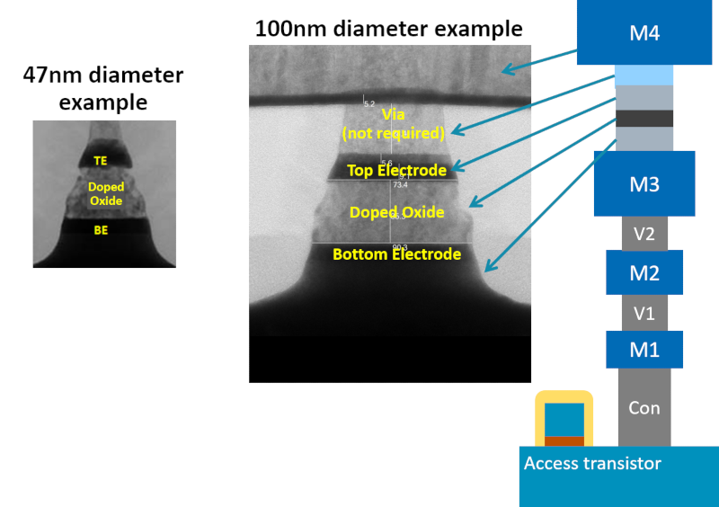
Correlated-electron RAM or CeRAM is the usual press release material. Nonvolatile, smaller than SRAM, and fast. It sounds as though it could replace the SRAM in PC caches, for example, and take up less die space on the CPU chip. The principle is a bit odd. When electrons are forced together in certain materials, the properties of the material can change. This Mott transition (named after the inventor [Neville Mott]) can take carbon-doped nickel oxide and switch it from its natural electrical insulating state to a conducting state and back again.
Whereas a traditional static RAM cell requires up to six transistors, a Mott cell is just a bit of material and one transistor. Speedwise it seems devices exist with 2ns write cycle, something they expect to get better with more work. We’ve read that the material changes state within 100 femtoseconds. There are some other tantalizing features. The memory appears to work at very cold temperatures (like, cryogenic temperatures) and very hot temperatures, as well. It also may be radiation resistance and can be made to operate on very low voltages.
The new company doesn’t plan to actually build devices but wants to develop the technology to the point that a major manufacturer will take over the technology and bring it to market. There are doubtlessly many hurdles to putting something like this in real production and it is yet unknown if the devices can be written to repeatedly without degradation.


“Correlated Electron (Ce) switches operate via strong electron orbital interactions, with a key example being the predictions of metal-insulator transitions by Nobel Laureate Neville Mott over 70 years ago. ”
Seventy years ago. man what history could have been.
“The entirely new switching physics that has been harnessed in these new materials begs investigation into a wide variety of additional applications beyond memory. These include analog neuromorphic applications, RF applications, sensors and even “beyond CMOS” switches”
And then there’s the kind of stuff that makes this forum giddy.
Wait and see…
Yet another groundbreaking, “1-transistor wonder” that could and should be seen everywhere :
https://www.cpu-world.com/CPUs/680x/Motorola-MC68701U4S-1.html
But we’re still waiting…
I must be missing something. You have linked to a page for a 1 MHz microcontroller in a DIP 40 package. Is that what you’re still waiting for?
Are you suggesting that one is available?
B^)
I developed this rule: “when in the title of an article there is a question mark ‘?’, 99% of probability that the article is pure crap/advetisement or other kind of shit that does not deserve my time”.
A bit like the show business adage that productions with title ending with an exclamation mark are doomed. Oklahoma! may have been an exception.
Oh! Calcutta!
Kiss Me, Kate!
Oliver!
Hello, Dolly!
Mamma Mia!
You reinvented the Betteridge law of headlines: https://en.wikipedia.org/wiki/Betteridge%27s_law_of_headlines
Mine is a bit simpler/shorter: If the title contains a question mark, the answer is No.
If my daughter asks a question*, the answer is “No!”.
B^)
*usually pertaining to money.
you aint replacing sram any time soon, it has really low latency which is why its the ram of choice for cache. they are willing to put up with its hugeness and high cost because of this. unless this new tech can beat that latency by a significant margin it wont be replacing your cache any time soon. any memory that can be both as low latency as sram and denser would probably replace it as soon as it was viable to do so.
Not to mention that SRAM has the huge advantage of not needing any additional manufacturing steps. Since it uses the same transistors as the rest of the logic.
So moving to another memory technology would likely add additional manufacturing steps, adding direct manufacturing costs and lowering yields, thereby increasing costs yet more.
I have seen some chips that have experimented with using DRAM for higher cache levels, but considering that it isn’t wide spread, then it clearly doesn’t seem to be worth while the additional manufacturing steps and lower yield.
And additional manufacturing steps have yet one more hidden cost other than lower yields. But the more masked layers a chip has, the harder it is to find manufacturing time for it. (Unless one owns the factory, but then one has to face the issues of scheduling production oneself instead…)
So outcompeting SRAM is a hard task to say the least.
The additional manufacturing steps here aren’t bad, which is the point. It’s completely possible to integrate into a normal manufacturing process.
But it’s less about targeting SRAM than targeting Flash: the article here neglects to stress that it’s *nonvolatile*. Also with no known wear out mechanism, since the write voltages are much lower (rather than the “damn you, get in there” charge forcing of flash).
Considering that a modern semiconductor manufacturing facility tends to only have between 5-12 machines at their quoted manufacturing node.
Then asking for 1 more can be a stretch, considering that just building transistors tends to consume between 3-14 of those layers, not to mention the first interconnect and via layers.
The rest of the chip uses progressively larger manufacturing processes. At times quickly doubling in size after just the first interconnect layer.
Though, I myself already know that this technology isn’t viable for cache. As I have outlined on a comment bellow.
Yes, obviously. This is targeting *high-end* fab, because they’re targeting *post-flash* nodes. At some point, it becomes impossible to do flash memory at a process node, because you just freaking run out of electrons. We’re basically at that point now.
In this case the added cost doesn’t matter because you *don’t have an option*. In some sense it’s just the cost of moving to the new process node.
Is this another example of the Ovshinsky Device?
http://www.rfcafe.com/references/radio-electronics/ovonics-radio-electronics-may-1969.htm
No: that was an ovonic switch, which is basically a super-early version of phase-change memory, which is basically Intel’s 3D Xpoint (well… according to everyone except Intel).
This isn’t a physical transition like that, it’s an electronic transition.
Here I sit wondering, what makes this special?
It is “different” than say 3D XPoint “memory”?
3D XPoint (aka Optane if produced by Intel) consists out of an oxide layer with a dopant in it, who’s conductance changes when one forces current though it.
If such a technology will be used for cache in a CPU is a bit unlikely, though L3 might be a candidate.
L1 and L2 is a bit too latency sensitive for such an application. Though, L3 is a fair bit active, so the technology would need fairly low dynamic power consumption for it to be relevant as L3 cache.
Though, using it for cache would also come with some rather major security concerns. Non volatile memory tends to be a bit “iffy” to deal with when security is needed.
Not to mention any long term failure modes to take into consideration.
And extra manufacturing steps, effects on yield, and other potential issues.
Also I find the statement “a traditional static RAM cell requires up to six transistors, a Mott cell is just a bit of material and one transistor.” a bit odd…
Most SRAM cells only really needs 4 transistors. A 6 transistor solution has some advantages in terms of speed, and we can actually build one with 8-10 transistors without having redundant transistors.
But one should not use a wasteful implementation of a technology as a comparison against another technology, it isn’t really logical after all. And using an “up to” in comparison to an “as little as” is rarely useful. (For example, wind farms can produce as little as 0 watts/m^2, solar power can produce up to 300 watts/m^2. Which one is better? (the example is meant to be stupid, no need to answer it))
Comparison to Xpoint’s hard because Intel’s super tight-lipped about how it actually works (so it’s hard to compare the *theoretical* limits), but it’s almost certainly faster, lower power and with higher write endurance and lower write latency. Pretty much everyone believes Xpoint’s phase change based (even if Intel doesn’t like the word, I guess) which means it’ll have finite endurance (and Intel’s Optane specs don’t match the “bajillions of write cycles!” claims in the press releases) and explains the decently high write latency.
Again, assuming Xpoint really is phase-change with an ovonic switch, you’re talking about programming energies in the volt/milliamp scale, whereas these are in the fractions of a volt/microamp scale.
“Not to mention any long term failure modes to take into consideration.”
That’s because there aren’t any. Flash fails because, well, you basically slowly burn the insulator between the control gate and the floating gate (yes, yes, not “burning”, I know, but “burning” sounds cooler). It wasn’t a surprise that flash fails after some number of writes: it’s incredibly obvious, because you’re forcing electrons across an insulator with a high voltage (well, high to a MOS structure, typically ~20V-ish). This was perfectly well known when they came up with it. Hence the reason why they have specs on maximum number of writes. It’s got a limited life, it *will* fail. Flash has write endurance in the 10^4-10^5 cycle range.
Similarly phase-change memory also has a limited endurance because of the thermal changes (go fig, functionally decrystallizing/recrystallizing stuff eventually destroys it). *Should* be much higher than flash, but still functionally finite. From what I’ve seen PCM/ovonic switch stuff is in the 10^9 range typically (although IBM’s demonstrated 10^12), but the Optane Xpoint memory is functionally identical to flash (~10^5-10^6). Given that IBM’s high-endurance requires additional process steps, this is likely a cost-saving measure.
Oops, forgot to explain why there aren’t any in this case – it’s because the transition’s basically just electronic (everyone says ‘quantum mechanical’ but it’s an electronic band structure change due to quantum mechanical effects). In the “conducting” stage, the nickel atoms have a conduction band so charge flows freely. However, if they gain another electron (due to an increased applied voltage), the extra electron modifies the band structure so the conduction band goes away. That’s the “conductor->insulator” transition, and that’s the “ludicrously fast” one, since again, it’s purely electronic.
The reverse (insulator->conductor) transition is slower: you basically force higher voltages and rip off those extra electrons. This is slower, but still very fast (nanosecond-scale). And again, since you’re not actually physically *altering* anything (like, forcing electrons across an insulator, or rearranging lattice structure), it’s adiabatic – there’s no wear mechanism specific to the memory itself.
3D XPoint we don’t know too much about. Unless one reads the patent that spills the beans on it, otherwise it isn’t a valid patent. (And I am going to guess it is a valid patent, otherwise the technology is just a trade secret, and other companies are practically free to reverse engineer it and built it too.)
If you can’t recreate the technology through the patent alone, then the patent doesn’t cover the technology. The only thing making other companies illegible to produce the product is legal enforcement of the patent. (Now a patent doesn’t have to go into how to manufacture it, it just has to outline the finished product.)
I am also curious to how you know the programming energy of 3D XPoint if you don’t know how it works, all though, it could be estimated by looking at the power consumption of the chip itself, even if that has a large margin of error due to other on chip facilities drawing power.
And in regards to “there’s no wear mechanism specific to the memory itself.”
Changing the valence electronics of an atom tends to change its crystal structure rather dramatically.
That is why I say, “how is this different?” other then the obvious use of other materials.
(I could also take a detour into micro scale crystal structures and how they tend to bond together and form monocrystalline structures if left to their own devices.)
Also, in regards to Flash endurance, it is closer to 10^2-10^6 depending on the manufacturing process behind it. (It tends to be towards the lower end if built for density, like the flash used in SSDs. Ie, one shouldn’t look at Microchip’s endurance specification stated for the flash in their microcontrollers. (Since Microchip has phenomenal endurance in their flash, but it is however far from dense…))
Then there is also the question of the stability of the material in each of its phases.
Memory retention is a rather worth while thing to look into. Flash is currently around 3-100 years, depending on the process. (Microchip specifies their flash at 80+ years at room temperature. While commodity SSDs are likely closer to 3 years…)
But any chip tends to fail out in the field regardless.
Though, flip chip technology has a nasty habit of the connection between chip and carrier/board being the thing to fail due to thermal cycling, and not the chip itself…
“3D XPoint we don’t know too much about. Unless one reads the patent that spills the beans on it, otherwise it isn’t a valid patent.”
OK, I’m guessing you don’t know about the hilarity of Intel/Micron insisting that 3D Xpoint isn’t PCM? That’s the reason for all of the “maybe it is, maybe it isn’t??” Micron previously attempted to sell PCM back in the mid-2010s, but had to pull it (because… it didn’t work). So when 3D Xpoint came out and people were like “isn’t this PCM?”, Micron comes out and says “nonono! This is totally different!”
Then 3D Xpoint came out, and people decapped it and scanned it… and it’s PCM. So why, exactly, would Micron/Intel be so “it’s not PCM!” when it clearly is? Legal crap. There’s some shady patent shuffling which happened right before 3D Xpoint came out, which Intel/Micron are still in legal issues over. (The company they’re in legal trouble with? Ovshinsky’s company. Yes, that Ovshinsky. See above comment.)
“I am also curious to how you know the programming energy of 3D XPoint if you don’t know how it works, ”
Because it *is* PCM, but you have to put in this wavy-hand disclaimer because Micron swears it isn’t.
“Changing the valence electronics of an atom tends to change its crystal structure rather dramatically.”
It’s a quantum-mechanical effect. The available orbitals are always there: it’s just that when they’re poorly populated, the band energies are such that it becomes a conductor. When they’re highly populated, the energies split (due to electron spin splitting), and that same conductive band goes away.
It’s easy enough to understand why it’s non-destructive: the Mott phase transition occurs in *femtoseconds*. There’s literally no time for any physical change to happen. The *reverse* operation takes longer (nanoseconds) but again, because you’re applying such a low voltage, the actual stress to the device is minimal. Obviously there *will* be some upper limit at *some* point (certainly with process scaling).
“Also, in regards to Flash endurance, it is closer to 10^2-10^6 depending on the manufacturing process behind it. […] (Microchip specifies their flash at 80+ years at room temperature. While commodity SSDs are likely closer to 3 years…)”
You’re mixing NOR/NAND flash. Yes, NOR flash is closer to 10^6+ (and the ’80+ year’ lifespan you’re quoting), but density-wise it’s so far from the game that it’s not worth talking about it. No one’s building multi-gigabyte SSDs out of NOR flash. NAND flash is better thought of as 10^4-10^5 best case, with mult-bit per cell being much lower. And obviously with multi-bit per cell NAND flash, unpowered data retention is much lower due to the far smaller margins and thermal degradation.
“The principle is a bit odd. When electrons are forced together in certain materials, the properties of the material can change.” Not really odd. Chemistry is all about electrons. And then there is the periodic table.
I would think that even if it doesn’t have theoretically optimal speed or density, that the materials it is made of might make this an attractive technology. Carbon and nickel aren’t too exotic or expensive.