[Billy Wu] has been writing for a few years about electrochemical 3D printing systems that can handle metal. He’s recently produced a video that you can see below about the process. Usually, printing in metal means having a high-powered laser and great expense. [Wu’s] technique is an extension of electroplating.
Boiling down the gist of the process, the print head is a syringe full of electroplating solution. Instead of plating a large object, you essentially electroplate on tiny areas. The process is relatively slow and if you speed it up too much, the result will have undesirable properties. But there are some mind-bending options here. By using print heads with different electrolytes, you can print using different metals. For example, the video shows structures made of both copper and nickel. You can also reverse the current and remove metal instead of depositing it.
This looks like something you could pretty readily replicate in a garage. Electroplating is well-understood and the 3D motion parts could be a hacked 3D printer. Sure, the result is slow but, after all, slow is a relative term. You might not mind taking a few days to print a metal object compared to the cost and trouble of creating it in other ways. Of course, since this is copper, we also have visions of printing circuit board traces on a substrate. We imagine you’d have to coat the board with something to make it conductive and then remove that after all the copper was in place. When you build this, be sure to tell us about it.
We’ve seen electroplating pens before and that’s really similar to this idea. Of course, you can also make your 3D prints conductive and plate them which is probably faster but isn’t really fully metal.


Urg I’ve been working on this in my garage for 6 months now :(
Well, my technique is a bit different, still this is pretty annoying, why does this keep happening. Next week you’ll have an article about somebody building a giant dome 3D printer like the one I have half-built too :(
Guess I need to work faster.
I wish everybody but me would stop doing innovative crap :)
Improve, make easier to replicate, and publish. What is shown here is still a long way from being something that an average hacker could easily reproduce, let alone buy ready-made.
But the speed issue may be significant. I wonder if there is some clever chemistry way to activate electroplating solution using light – then ordinary resin printers could be repurposed for metal printing.
Mhm, I’m using a laser, there’s lots of research on that around, just not applied to 3D printing. My goal is to work this into something people can adapt on existing lasers or CNC mills as a kit, so I guess that part of the project still makes a lot of sense to do. First need to make it actually 3D print though, which I don’t have working correctly yet.
Copper Electrodeposition for Nanofabrication of Electronics Devices by Masayuki Yokoi (auth.), Kazuo Kondo, Rohan N. Akolkar, Dale P. Barkey, Masayuki Yokoi
You could use a dry method like using a kind of small high voltage Ion thruster with copper particles getting ionised and deposited on the material I guess right? This would be cool because you could use this to fuse and remove material too by adjusting current, voltage and feedstock. The electrolyte thing looks kinda sketchy because it would take stupid amounts of time to have nice coatings and In don’t know if there will still be quality issues if they use high currents…
I would not use this method ever except for small circuit making like boards and stuff.
You could stick that on a cnc machine I bet as you could tweak the electronics and have already the high custom capability of cnc machines like drill bit speed could be repurposed to be current or something!
A corrosion resistant chip with say 0.5mm sized switchable electric-contact-pixels would multiply the print-speed by the number of pixels. This is still quite slow but still orders of magnitude faster than just one pixel at a time.
To minimize stray deposition the chip would need to be much closer to the printing plane than the size of the pixels. Say 0.1mm.
Just constant voltages or even constant currents may not cut it due to eventual unstable instabilities in deposition rates and accumulated deposition heights. Currents for constant voltage need to me measured and adjusted currents for deposition need to be set in order to get the deposited surface back to planar again. All that on a per pixel basis. Here the stray currents help blurring things out.
Pixels at the xy-to-z-edges of the so far accumulated 3D print (concave straight or convex corners in the xy plane) would need special treatment. I’d suspect fundamental geometry limits since stray currents always go down a bit the side flanks of the so far accumulated print.
The Chip probably needs to be sufficiently heat conductive and actively cooled on the back-side to prevent electrolyte overheating and boil-off. Maybe a peltier element? A good thing is that electrolyte layer thinness helps massively to reduce resistive losses.
Also the Electrolyte needs to be refreshed somehow given the minuscule volume between accumulated print and the pixels (0.025mm^3 here). A slow and easier way to do this would be a periodic lifting of the whole chip akin to the action seen in resin printers. A fast and difficult method would be blow-in of Electrolyte through holes in the chip. What would be the speed bottleneck here? Repeated lifting or depositing.
Well obviously one could play around wit an added AC component, cooling near freezing, ion chemistry, solvent chemistry, … to try going a bit higher with the current. But this most likely won’t gain many orders of magnitude speedup and reduce print quality.
Unfortunately all this including highly parallel individually controllable high power electronics and simultaneous backside cooling (unfortunately faking parallelism like done in many displays is not a viable option here)
seems very challenging and currently pretty much beyond what can be done DIY.
Maybe I’m wrong …
My rule of thumb at work: “If the project timescale is more than 6 months, it will be out of date by the time you’ve done it”.
I’m poor and busy enough that the project timescale is way more than 6 months unfortunately :(
Guessing you’re THE Arthur Wolf, Smoothieware creator? :)
Hey Lerche1989, long time :)
Yes that’s me. And I want to make something clear, this whole thing about working on a new 3D printing tech, is something I haven’t put a lot of time into, mostly because I am so busy with Smoothieboard v2. It’s not taking time away from Smoothieboard stuff and other responsibilities I have to the community. It’s something I had an idea for, and I put some effort into when I can, which is rare.
Smoothie was designed to make these sorts of “weird” applications possible, by the way, and I feel like it’s helping me accomplish this easier than if I didn’t have Smoothie as a tool to do it.
Also, as I do Smoothie stuff (dev, documentation), I need to keep in touch with what it means to actually use the system (that’s where a lot of the ideas for improvements will come from for example. Or how bug finding happens etc), so projects like this are actually good for the Smoothie project, I feel.
Anyway, just making sure nobody thinks I’m abandoning the project or anything, this is meant *as a part of* my normal duties as the Smoothie project community manager/project creator.
Hopefully I can get this technique to work, and maybe make like a kit with a Smoothieboard, some of the hardware needed for the electroprating, and lots of documentation/software so others can also play around with this technique.
I feel like metal 3D printing is one thing our DIY/maker world is still missing easy access to, and I’ve worked a lot on trying to find ways to make it more accessible (for example helping with a lot of efforts at making open-source DMLS setups over the years), and this is my attempt at taking a chance at maybe making some progress towards DIY/open-source metal 3D printing for the community.
Sorry for rambling.
An interesting ramble like that can definitely be excused!
While I have to admit I’m a little impatient for the new smoothie, as I’ve got projects in mind for them (a few any similar board could do, but I don’t have any of those spare either… ), taking the time to do it right is important, and part of that is taking the time to look at and think of other things – no use to the projects you’re part of if you’re burnt out, or so focused on one little bit you miss the obvious opportunity to make/develop a part in a better way…
You’d like to stifle world progress for self gratification! I think you’re the kind of guy who’d like a hollowed out volcano, minions (people or yellow type) and daily opportunity for an evil laugh :)
We can dream…
Obviously I’d like things to move as fast as possible in the direction of progress. It’s just frustrating when I think I have a cool idea, I spend hundreds of hours on it in my garage with a near zero budget, get close to something that works, then some big university somewhere else in the world publishes about the same thing right when I’m close to having it working.
Just saying it’s frustrating for me personally, even though obviously it’s a good thing if you take a step back.
It’s like that time I had 300 BTC in a wallet and bought dumb stuff online with it, or that time I coded something *very very* similar to Minecraft a year before alpha came out, but never showed it online because I thought it sucked, both true stories.
Hopefully at some point I stop being dumb and/or unlucky.
If it makes you feel any better, I’ve blown over 10 BTC and a few hundred LTC on stupidity, tossed out several pieces of Apple II hardware when it was in the valley between useless old junk and cool vintage stuff, lost a $5000 MTG card, forgot/declined to develop and patent a GPU “physics processor” in the late 90s because it seemed too obvious, and possibly passed up a large box full of Group of Seven artist “sketches” because it didn’t dawn on me that real artists would paint on hardboard.
Well, we’re both dumb. Not sure this helps either of us in any way :)
Yah, just gotta Edith Piaf that stuff…. https://www.frenchlyricstranslations.com/non-je-ne-regrette-rien-edith-piaf-french-lyrics-and-english-translation/
check out some of Frank Frazetta’s work — He did one piece in masonite since he was out of canvas and painting was due next day! His wife described that process to me with a fair amount of detail on one of my trips to his museum.
Losing your first million is always the hardest. Best get it out of the way quickly.
Arthur, so you didn’t get the scoop, and I bet a few other big universities somewhere are cursing they didn’t get the scoop. Keep on doing your research and development at the pace you can, you’ll still make a valuable contribution.
(Sorry, I accidentally ‘reported’ one of Arthur’s comments looking for the reply button…)
Count the successes though…there are many. And also realize you are doing this out of your house, not a university.
This is not a new problem…it extends back in history over many major inventions and just about every biography I read I hear about how someone was working on the same thing at the same time. Maybe it is just the way things are presented to us….maybe it is some form of synchronicity.
But also, never forget Feynman’s story https://www.dovgordon.net/how-feynmans-phantom-lab-faked-the-competition-into-folding/
Keep working…you never know what you will stumble on that they didn’t.
:’)
I’d say that a smart way to do something similar albeit with some high costs would be to do some kind of simple ion thruster and yeet inside a hot metal bar that would ablate and deposit a small steady stream of ions on the surface. You could also take away material by replacing the bar with argon gas or something like that.
I have similar problems keep happening in my last 7 years – mostly on the lasers and cnc fronts. This last year I’ve been thinking that I need help, that I need to team up with others like myself, I just don’t have enough time and energy to bring some larger ideas to life fast enough or good enough.
Thanks for your work btw, much love, do you have a patreon? I’d totally donate to you.
I totally want to start a patreon, many people have said they’d help there, but I don’t feel comfortable doing that until I have fullfiled/shipped the boards from the Kickstarter for Smoothieboard v2. But thanks it really means a lot to me that people would be ready to donate. And would change a lot for me if/when it happened.
If you need help with the electronics side of things, don’t hesitate to ask. If you’re doing something innovative or that somehow helps the community, we can even send you a free Smoothieboard depending on the project.
I was involved with research on this some 20 years ago, it was abandoned due to slow deposition rate, it may find applications in antenna, micro area.
I’ve found some ways around that, there’s been a lot figured out/published lately. Hopefully, I don’t have anything actually working yet.
Yes, I imagine progress has been made, a simple low resolution concept may be to have metal spheres, say ball point pen size, deposit down tube, then spot weld to substrate or previous deposited spheres.
start with single depositor then use array, the result would be poor surface finish which may be infiltrated.
resulting part should be strong.
Small metal spheres you say? Can make a 2km wide funnel out of cheap tarps duct taped together, lift it up with V8 powered octocopters around the edge, and catch micrometeorites to 3D print with. :-D
Dude same shit happened to me except I was building super efficient feul generators
Don’t worry, it looks like it’s pretty early days for their tech. I’m sure they have a very long way to go to make it really usable. I noticed they don’t have a single photo of their actual setup, which is a bit strange, but maybe it’s not very photogenic.
Happened to me a few times. 😞. It sucks. BUT at least if you get yours going, you’ll HAVE it, be able to do things with it, and will maybe will have some improvements in your version that avoids some pitfalls of the “published” version. And YOU did it! So you didn’t get to yell “first”, maybe yours will work better/faster.
I think this might be missing the point of electroplating. It is very good for large surfaces. So why not flip this on its head. Print a mask, submerge in plating solution, and plate the entire layer in one go. Perhaps the print bed can lower into a bath of solution and then come back up for the next layer. Then print your next mask directly on top. Repeat. At the end, you’ll need to remove the mask, but with a metal part that should be easy with chemicals and/or heat. This would move the bottle neck to how quickly can you print your mask and ready the layer for the next round.
Shhhhhhhhhhhhhhhh!
I saw a film from the 1970s showing how Tektronix built multilayer boards with through-hole plating, using this technique. So it’s really not a secret.
https://www.youtube.com/watch?v=7weZ0TNRcuw
If you add resin to the solution and cure it via UV light like in SLA you could get it.
How is the next mask supported by the previous mask/copper layer?
conductive masks
It’s masks all the way down.
Apologies to Science fiction writer
Terry Pratchet.
It’s when you try to do something this that you realize the Faraday Constant is a real beotch.
It takes a *lot* of ampere-hours to deposit a few grams of material. Just the electricity can cost more than your feedstock material, at least at anything larger than hobby scale.
The cost-benefit is not with your value of volume of material, but with alternative processes to get competing results: print-in-place jumbo-mems widgets that can’t be produced any other way is an attractive idea
In my experiments with electroplating, it hasn’t taken nearly as long or nearly as much power as I would’ve guessed. I even made a little plating-circuit that runs off of 4 AAs. It could run off of one for hours if I’d had a boost converter lying around.
I played with copper sulphate solution in school and one way of dissolving more copper sulphate is to increase the temperature of the solution. Of course if you pass boiling point it will evaporate and if you increase the pressure to lncrease the boiling point it will be difficult to work with. maybe there are other solutions than water with a higher boiing point.
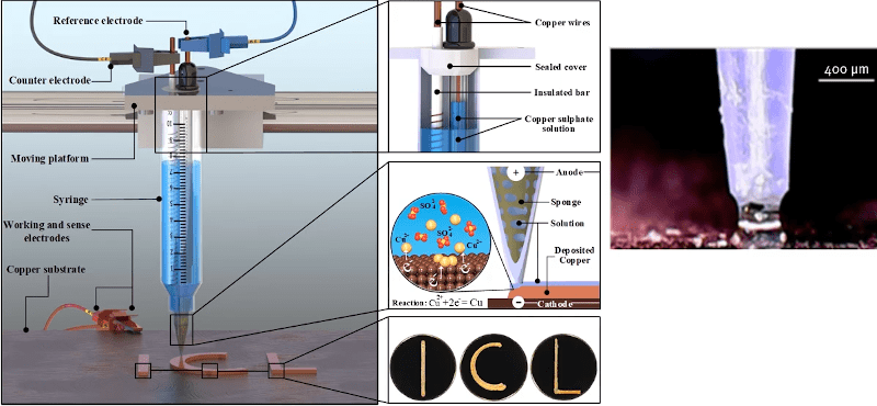
The speed issue seems quite significant. To quote [Wu]: “Unfortunately this approach is a quite slow for large objects. In our previous paper we showed that for a 400 μm nozzle, we can achieve a deposition rate of 20,000 μm3/s. So for a 10 mm cube with a 10% infill that would take approximately 58 days to complete. There are a few things you can do to accelerate this, but this is the reason why this is still mostly at the R&D stage. However, there are applications for smaller scale structures which are electrically conductive.” https://www.youtube.com/watch?v=B-UbDk7LrvU&lc=UgxGfbJ17uFK2mqjyjF4AaABAg.9IHpscIkSTo9IINo7LdiSm
The obvious answer is to parallelize it. Instead of a single 400 um nozzle, you could have a linear bar of a few hundred of them, running like a page scanner.
Then you realize that still doesn’t buy you that much speed, so you design a massive 2-D matrix of a million nozzles.
Then you realize you’re running running kiloamps through it, and still only get a fraction of a millimeter per hour of build speed…
But you can then make a few exotic widgets that no-one else in the world can, and someone decides they need them for something, and bingo, you’re rich.
For reference, my single-threaded electroplating is current limited at 0.03 A (probably higher than it should be). A million electroplating heads could well be kiloamps…but 1000 heads at 30 amps isn’t that scary.
So you’re suggesting a copper jet printer.
Crank up the current, add laser light to the jet, add ultrasonic thingies, lots of ideas in the literature about speeding up electrodeposition, I’m sure they will try some of them.
If you want to make a circuit board, it would be much better to start with a copper clad board and remove what is not needed via electrolysis, rather than make a conductive base, deposit metal traces, remove them in some miraculous way without destroying them and then fix them to a nonconductive surface.
Agreed, though with the 3d plotting abilities this has a home brew of those 3d PCB plastic type things that exist in phones and the like, perhaps with even more impressive geometry could be done.
I was part way through this idea after watching an applied science video on it I think. And thinking on it again now having just seen this, it seems like a SLS resin applied by needle to be rapidly cured might be a good choice for this idea – multiple syringe in the printer apply the resin layers, leaving channels for the electro-less solution to pool in, then electro deposit on those lines (and use the electronic step to tidy up any overspills), build them up as much as you like moving back and forward between resin and the conductive solutions (keeping electro-less plating solutions stable for long is tricky, which is the main area of concern I had with this idea).
Or, instead of electroplating, use the syringe to ‘salt’ areas of the substrate with chemicals that will plate up metal through chemical reactions.
‘Electro-less’ nickle and copper plating is how plated-through vias are made!
Or perhaps even better, develop filaments that are ‘pre-salted’: after printing, immerse the substrate in a plating bath, metal deposits only on ‘salted’ traces without the heat and bubbles of using electricity.
I really like the idea of removing metal for very fine work!
Bonus: any metal stripped from the substrate gets ‘plated-up’ on the syringe electrode: all the metal is reclaimable!
Fill your laser printer with metal powder and quadruple the voltage to the fuser, pass your piece through as many times as it takes to build the height you want :-D
Talking about metal powders, one thing I’m currently trying (I have the hardware done, just need time to finally turn it on), is to add copper powder to the fluid, with the hope that this powder will get “caught” in the electroplating as it happens, increasing the rate of deposition compared to using only the copper that’s dissolved. I’m really curious/hopeful this will work to help increase the deposition rate. I’ll make like a Youtube video once this is tested, and I guess give HaD a tip about it. This is exciting stuff, even if it’s pretty likely it’ll fail.
That sounds like a very plausible method, if you can keep the powder in suspension in the feed stock long enough.. If it all falls out away from where you are trying to plate, or jamming the works up it won’t do you any good…
I wonder what the conductivity will be like, as I’d assume with the powders you might end up with ‘little’ cavities around them that are from an electrons point of view enormous…
This is how nicasil coatings are applied. Fine silicate powder is held in suspension by agitation of the plating solution as the nickle is plated onto the component. Other powders and metals may be susbstituted.
Shhhhhhhhhhhhhhhh
That’s indeed the sound copper powder makes as I pour it into the solution :)
Seems like this approach would rock as a “solder” builder for a wire tack/ feed machine.
Have a wire feed welding tip, an electro depo tip, and a roller tip of non-conductive epoxy,and a extrusion nozzle of nc epoxy working on the same layer.
You could build traces with the wire, track around vias with epoxy nozzle, and inject with the depo tip to build up via connections, then layer nonconduct with rollers around and over areas that need to insulate, and fix that epoxy with UV.
this would work great in microgravity to build 3D processing cubes, with large “wells” going to the center for heat removal.
Those wells can be filled with opened benzene, which acts like zig-zag graphene, as an electro-thermal conversion sink. Pull heat out as eV, like the new phonon conversion processes. ASU did the benzene work, but never connected it to the graphene.
Working on opposite sides of the cube, allows multiple heads to work on different sides, to avoid interference, and help with speed.
2-D edge work.
I keep thinking this could be used to “solder” components on PCBs using copper instead of the normal solder paste methods, but I can’t figure out exactly the way it’d work. It does feel worth trying out/investingating though.
Proper masking, and a willingness to rework with the fiberlaser resulted in a few successes electroforming parts in place but undesirable interactions between the plating current and components lead us to abandon our efforts.
we had mixed results in adding nano powders to our process. While it did speed our deposition rates, in almost all cases it resulted in undesirable voids and inclusions in the parts. Our primary use case cannot tolerate these issues but perhaps yours would. While copper/nanocopper didnt meet ANY of our requirements, We did get some very useful samples of tungsten/nickel, tungsten/copper, titanium carbide/nickel, and titanium carbide/copper composites.
Everyone else in the comments seems to be chasing speed,
We are currently using asymmetric alternating current, we actually sacrifice speed for grain diameter, so our experiences may not align with your goals.
Try not to get discouraged, Remember that the bulk of the USPTO database arent completely new technologies but rather improvements upon others. Take what theyve shared of theirs, add it to what youve already got, and keep working. There may be an improvement or tangential development lurking ahead if you just stick with it.
Good Luck!
My take on this was to submerge a 3D printer in a fish tank of electrolyte and feed in copper wire as you would feed in filament. I considered using a carbon film as a conducive release agent and a shroud to confine the currant to a smaller area of the work piece but it ended up as a half finished shelf project. In theory the resolution, at least in the vertical axis, could be incredibly precise. You could also run it in reverse and subtract material. Perhaps have a loop of wire running through the head on a roller to collect the removed metal, so it gradually gets thicker, winding from one spool to another.
How does one get the product off the substrate? Laser, mechanically, reverse plating, water jet?
There’s an xk….Far Side for that… 3/11/88 “Secret Tools of the Common Crow” by Gary Larsen.
cant speak for OP,
we coat our deposition field with a conductive ink. It takes slightly more force than an msla print to separate the parts from the tray as a result.
Regarding these dendrites forming at higher voltages. What are the time scales to form these dendrites? Can you pulse high voltages ? What happens then ?
This is not a generic 3D geometry printing method, in fact it is best suited to the examples that were shown, funny about that… All of the geometry is just 2D with an extrusion into 3D and the additional important ability to change the composition along that axis.
Here is a new advancement in existing technology by Bilal et al.
High throughput electrochemically driven metal microprinting with multicapillary droplet cell
https://www.sciencedirect.com/science/article/pii/S2352492821000453?via%3Dihub
This is a very interesting article. I wonder how this method stacks up against Selective Powder Deposition, which is my favourite low cost metal 3D printing technique.
One limitation of this technique appears to be that you can only print elemental metals, and to make an alloy would require multiple print heads and complex printing sequences. For example if you wanted to print stainless steel is that possible with this technique? If be interested to hear your thoughts.
I wonder if you could print an alloy, such as stainless steel, by using that alloy electrodes?
Part of the magic of alloys is the size and shape of crystals of the metals in them and compounds of pairs, and grain structure. This is pretty darn hard to achieve without specific cooling profiles from the liquid state, even if it is just cool naturally in air. So it might not be possible to print these alloy structures, as one fragment of pure metal may kinda fuse to another, but it’s not forming the right crystal structure until you make it hot and sloppy.
Fascinating, appears “eminently doable” with “.. a heap of potential augments offering new material compositions..”
Thanks for post :-)
Didn’t actually see a demonstration of it in the video, maybe I missed it. The picture they show seems to have structures a few millimetres thick. From what I can tell, this might have taken a very long time to “print”? Until I see a video of it actually “printing” one of these objects I will assume that the picture was a “mock up”.
I think this would be great if we can use it to add embedded circuit traces to 3d prints. It’d be even better if we could use the resultant solution from chemical etching of PCBs or dissolving copper into some basic household etchants as the electroplating solution. Vinegar or hydrochloric acid makes Cupric Chloride which can be used to electroplate: http://www.docbrown.info/page01/ExIndChem/electrochemistry06.htm
This would allow small circuits to be made using a modified 3d printer with simple home-made materials. Someone could use this to prototype, then they could etch batches of PCBs if needed. It’d also allow folks to recycle the nasty copper-infused results of etching which is always a problem to dispose of safely and correctly.
Never seen anything like this method before. Interesting! Good review of the methods in general also.
Would be interesting to see a solar 3D printer like the one used for fusing sand, printing metal using the laser like melting method.
Nothing was mentioned about how to remove the finished print from the bed. With a normal plastic FDM print, the bed can be treated with things like painters tape, hairspray, stick glue and so on, and sometimes the bed can be released and the print flexed off.
For metal, presumably the first layer must conductively and electrochemically adhere to the bed, which (I am only guessing) is going to be much more difficult than plastic FDM to remove, especially for low height prints. Is there some form of conductive ‘release agent’ which could be used here?
Conductive polymers.
Graphite table.
Other metal foil, latter removable by chemicfl etching.
Better yet, foil of the same metal, so you don’t have to remove it. You just have to trim around the base of the part. The foil can be glue-sticked to the bed.
cant speak for OP,
we coat our deposition field with a conductive ink. It takes slightly more force than an msla print to separate the parts from the tray as a result.