Many of will have marveled at the feats of reverse engineering achieved by decapping integrated circuits and decoding their secrets by examining the raw silicon die. Few of us will have a go for ourselves, but that doesn’t stop the process being a fascinating one. Fortunately [Ryan Cornateanu] is on hand with a step-by-step description of his journey into the art of decapping, as he takes on what might seem an unlikely subject in the form of the CH340 USB to serial chip you’ll find on an Arduino Nano board.
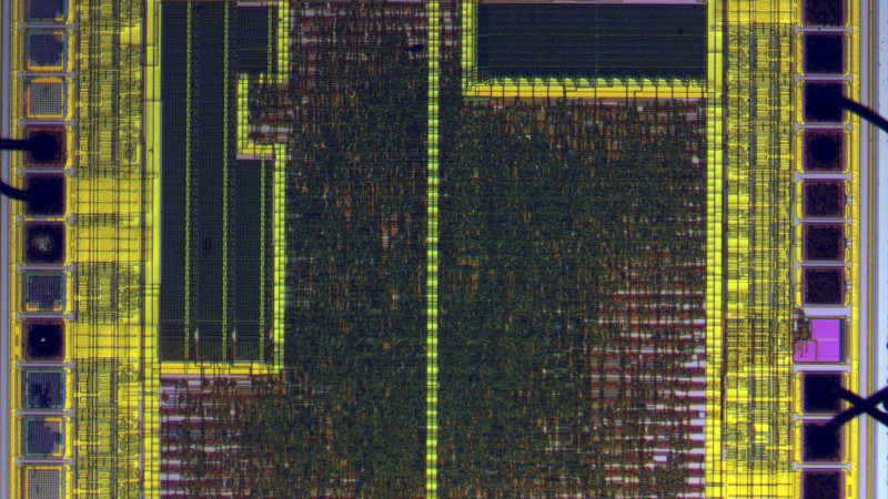
Starting with hot sulphuric acid is probably not everyone’s idea of a day at the bench, but having used it to strip the epoxy from the CH340, he’s able to take a look under the microscope. This is no ordinary microscope but a metallurgists instrument designed to light the top of the sample from one side with polarised light. This allows him to identify an area of mask ROM and zoom in on the transistors that make each individual bit.
At this point the chemistry moves into the downright scary as he reaches for the hydrofluoric acid and has to use a PTFE container because HF is notorious for its voracious reactivity. This allows him to take away the interconnects and look at the transistor layer. He can then with a bit of computer vision processing help extract a bit layer map, which with some experimentation and guesswork can be manipulated into a firmware dump. Even then it’s not done, because he takes us into the world of disassembly of what is an unknown architecture. Definitely worth a read for the armchair chip enthusiast.
If you’re thirsty for more, of course we have to direct you towards the work of [Ken Shirriff].


A nitpick:
“There are two types of metal typically used in the semiconductor fabrication process: aluminum (Al) alloy 6061 and/or copper (Cu) .”
I really doubt a structural alloy of alloy of alumnum is use for interconnects. As far as I know pure aluminum is usually used and sometimes alloyed with a tiny amount of copper.
The use of pure Aluminium would be fair crucial to be fair.
6061 contains 0.4% to 0.15% of copper and copper is literal poison as far as semiconductor junctions are concerned.
Aluminium on the other hand is a “weak” P dopant in silicone so will form a depletion region in contact with N doped silicone. (Ie, a diode.)
Copper though doesn’t really form depletion regions, and simply makes the silicone conductive. A great way to increase the leakage through a transistor, but rarely a desired trait.
Most chips don’t use copper for this reason. And copper isn’t all that much more conductive compared to aluminium, so not using it isn’t a major deficit. And it is primarily used in high power density applications.
Everything that isn’t high power density should preferably stay away from using copper interconnects since it is only increasing manufacturing costs for a slight decrease in interconnect resistance, something that at times can be fixed by just depositing thicker interconnects to start with. (Thicker interconnects isn’t always practical for various reasons, therefore copper is sometimes a better solution.)
But when copper is used on a chip, it will generally mainly be used on the larger interconnect layers, and then have a diffusion barrier when we transition down to our finer interconnects and eventually down to our transistors. But some chips have the diffusion barrier closer to the transistors. And some chips even encapsulate the copper traces in a barrier layer, but this at times risks eating up the whole benefit of using copper to begin with….
Though, the final metal layer can still see copper even on chips with only aluminium interconnects, for avoiding the purple plague if gold bond wires are used. But these days copper bond wires are more common. But bonding copper to copper is usually more stable than copper to aluminium, so copper pads is still nice to have.
Copper also has this awful property of diffusing really quickly. Even through things like glass and other metals like aluminium, so don’t use an aluminium copper alloy as interconnects… Though to the naked eye it is very slow at room temperature. But a sub µm thick obstacle is easily beaten if we give copper a few months to work on it. (most people tend to want their chips to run for a bit more than a few months, even at elevated temperatures.)
Tungsten/wolfram technically has the same poisonous issue as copper. But unlike copper, it doesn’t have much interested in migrating, being the metal with the highest melting point after all.
So yes, one would not use structural aluminium alloys for chips.
I should probably add why thicker interconnects isn’t always practical.
The answer is parasitic capacitance that would increase our switching load when driving the trace.
Another downside is more crosstalk due to more capacitance to nearby traces.
After all, the capacitance in a trace is directly proportional to its surface area. Making the trace thicker increases the surface area.
For higher speed circuits aiming at low power consumption. (for an example a CPU aiming at good power efficiency) then copper interconnects can be a very worth while investment, even if it reduces yields and introduces a literal “Chip on average dies in X hours of continuous use at Y degrees C.” to our spec. Since diffusion barriers are only slowing down the copper diffusion, not stopping it. Though, the MTBF value of a CPU isn’t really written on the box, but we can safely bet that the warranty period isn’t much shorter than the MTBF for 24/7 year round operation at peak operating temperature. (Since trimming down the margins in our diffusion barriers can lead to performance/efficiency gains that are more important up front.)
Is there a way to give them an individual serial number or such like with the tools for FT232R or CP210x?
Great work and great write up, all the better for not having a video attached. I am reminded of a rhyme my physics teacher uncle used to say:
Jonnie drank some water,
Alas, Jonnie is no more,
For what Jonnie thought was H2O,
Was H2SO4.
Poster in our school’s science classroom (from around 1999):
Johnny feeling life a bore,
Drank some H2SO4
Johnny’s father, an MD,
Gave him CaCO3
No he’s feeling very blue,
’cause he’s full of CO2
(the only reaction I can remember from school lol)
I am perplexed that the CH340 is not some 1T variant of MCS51 like other cheap WCH micros, but seemingly a PIC16F1454 derivative.
I hope through techniques like this we will (soon) know the contents of popular “black blob” chips. E.g. Broadcom, ESP32
Semiconductors use diffusion barriers.
Somebody at GitHub that is hacking about the JieLi MCUs, when studing about the F59 core architecture, states that has something similar to the PIC14 architecture (PIC16Fxxx), and also as the CH34x do (same PIC14 thing).