The early 1990s were an interesting time in the PC world, mainly because PCs were entering the zeitgeist for the first time. This was fueled in part by companies like Intel and AMD going head-to-head in the marketplace with massive ad campaigns to build brand recognition; remember “Intel Inside”?
In 1993, Intel was making some headway in that regard. The splashy launch of their new Pentium chip in 1993 was a huge event. Unfortunately an esoteric bug in the floating-point division module came to the public’s attention. [Ken Shirriff]’s excellent account of that kerfuffle goes into great detail about the discovery of the bug. The issue was discovered by [Dr. Thomas R. Nicely] as he searched for prime numbers. It’s a bit of an understatement to say this bug created a mess for Intel. The really interesting stuff is how the so-called FDIV bug, named after the floating-point division instruction affected, was actually executed in silicon.
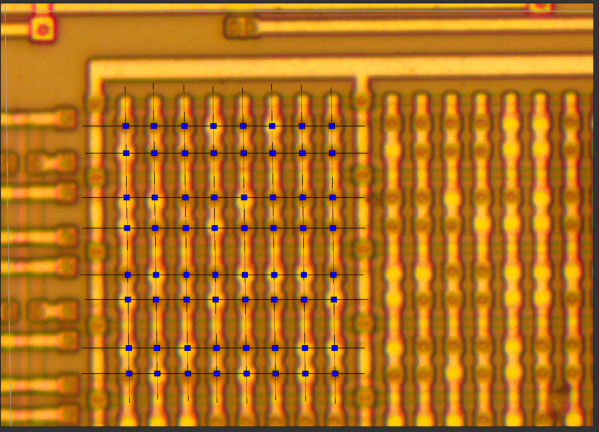
We won’t presume to explain it better than [Professor Ken] does, but the gist is that floating-point division in the Pentium relied on a lookup table implemented in a programmable logic array on the chip. The bug was caused by five missing table entries, and [Ken] was able to find the corresponding PLA defects on a decapped Pentium. What’s more, his analysis suggests that Intel’s characterization of the bug as a transcription error is a bit misleading; the pattern of the missing entries in the lookup table is more consistent with a mathematical error in the program that generated the table.
The Pentium bug was a big deal at the time, and in some ways a master class on how not to handle a complex technical problem. To be fair, this was the first time something like this had happened on a global scale, so Intel didn’t really have a playbook to go by. [Ken]’s account of the bug and the dustup surrounding it is first-rate, and if you ever wanted to really understand how floating-point math works in silicon, this is one article you won’t want to miss.