
These days, if you want to build something with modern chips and components, you probably want a custom PCB. It lets you build a neat and compact project that has a certain level of tidiness and robustness that you can’t get with a breadboard or protoboard. The only problem is that ordering PCBs takes time, and it’s easy to grow tired of shipping delays when you don’t live in the shadow of the Shenzhen board houses.
[Zach Fredin] doesn’t suffer this problem, himself. He’s whipping up high-feature PCBs at home with speed and efficiency that any maker would envy. At the 2024 Hackaday Supercon, he was kind enough to give a talk to explain the great engineering value provided by the Circuit Graver.
It’s always been possible to make PCBs at home. Many have experimented with irons and toner and etchant baths to varying levels of success. You can do great things if you invest in tools and upskilling, but fundamentally, it can be difficult to make good PCBs that do what you want. After all, there are a things that you might want out of your custom PCBs—fine traces a being prime among them. These can be challenging to do at home with traditional techniques.
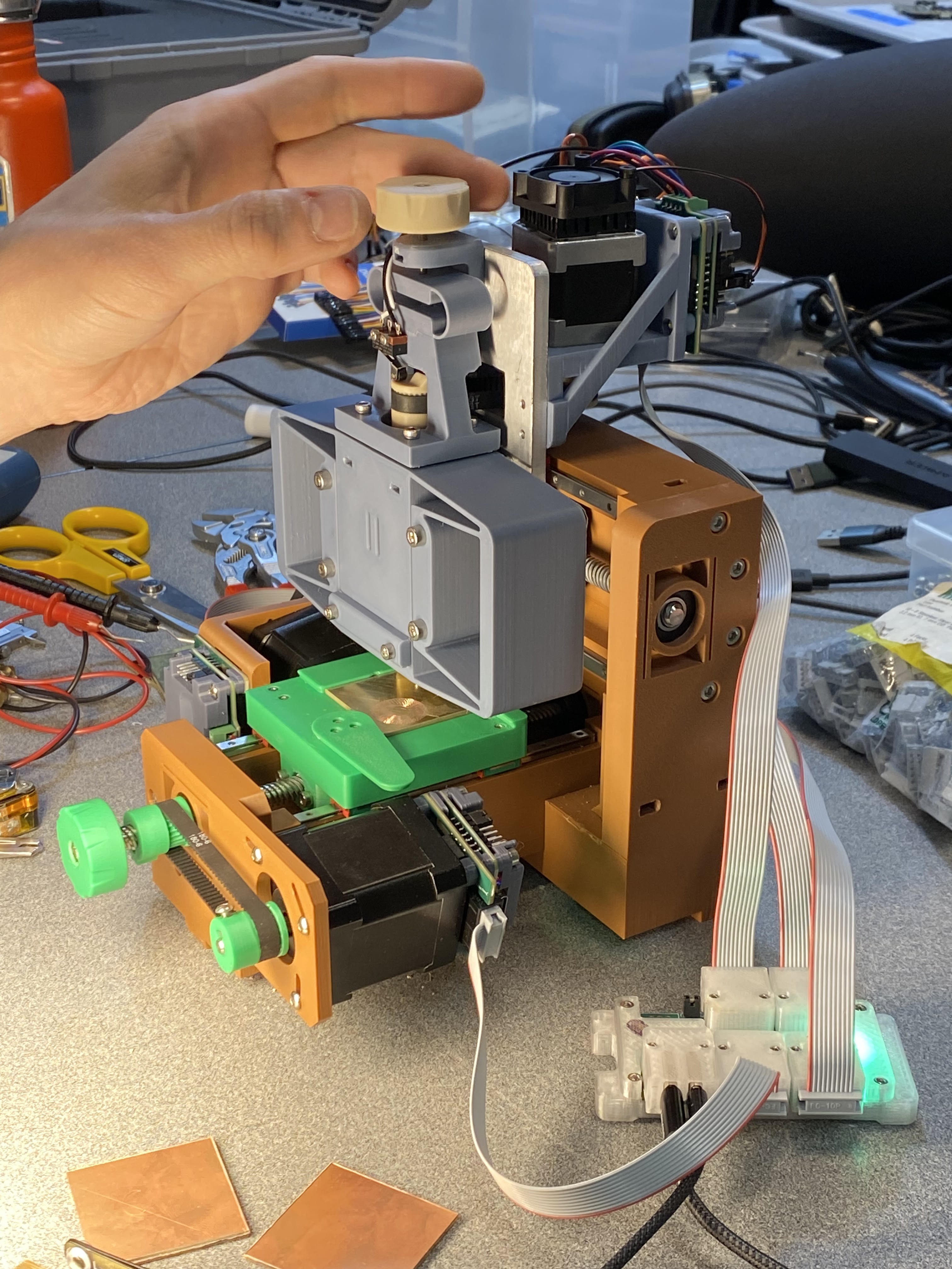
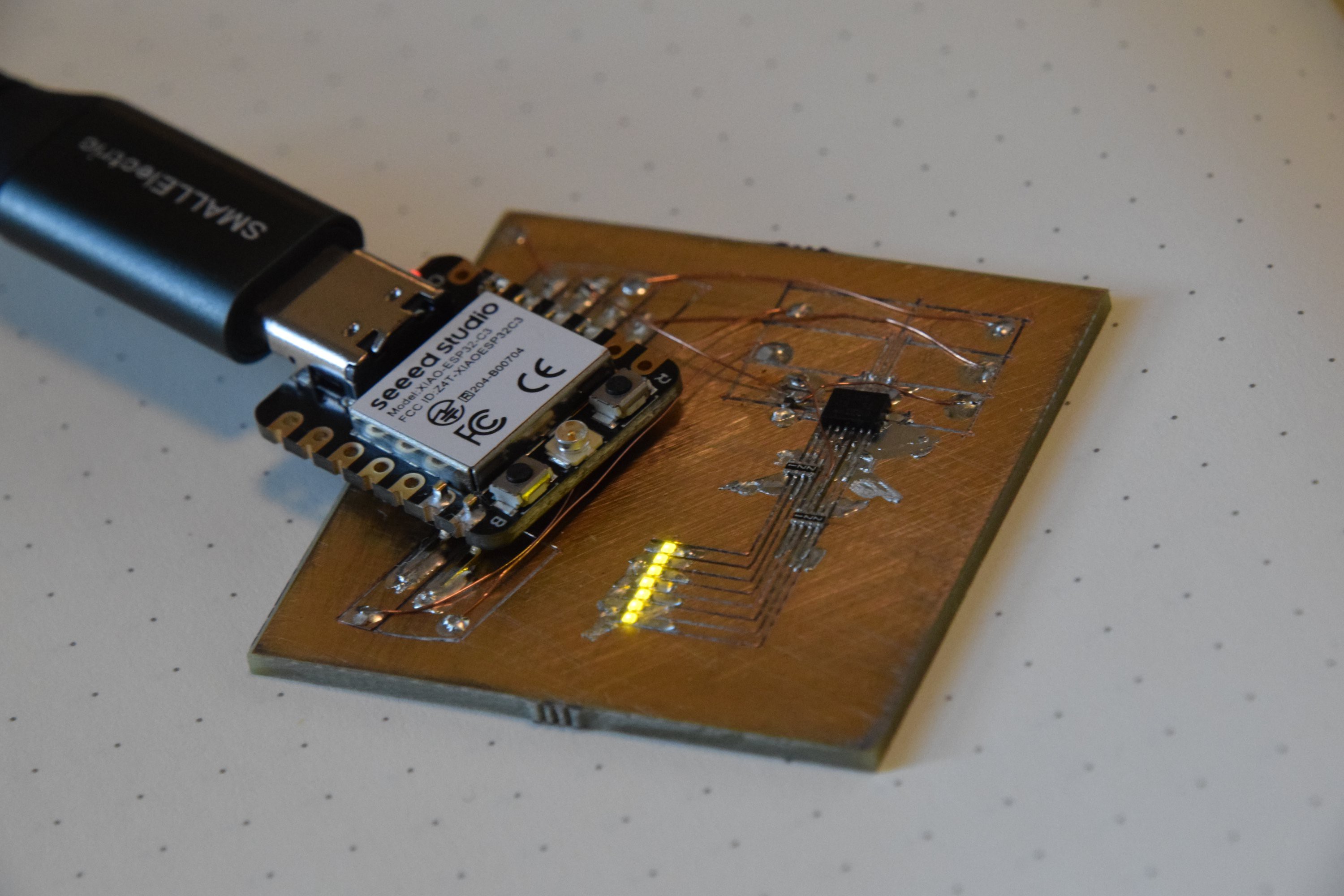
[Zach’s] focus was on finding a way to make these “high feature” boards at home—specifically, referring to boards with an excellent minimum feature size. Right away, his talk shows off an example board, featuring an 0.5 mm-pitch DFN chip, paired with 0804 resistors and 0402 LEDs. [Zach] made this board in his apartment, using a machine of his own creation—the Circuit Graver.
You might be expecting some kind of laser-etching machine or a PCB mill, but the Circuit Graver is a little different. Instead of a high-speed spinning engraving head, it uses a pointy tool to scrape copper-clad boards to create the desired traces. [Zach] was inspired to go with this route due to the limitations he’d found during his experiences with traditional PCB milling machines. He found them be loud, messy, and slow, and limited in their resolution. He’d found it difficult to build designs with anything smaller than DIP or SOIC chips when relying on milled boards.
The Circuit Graver was spawned by a technique [Zach] developed years ago, when he started carving boards using a modified box cutter blade by hand, before realizing the same technique could benefit from the magic of Computer Numerical Control (CNC). Rather than move the tool yourself, why not have the computer do it more accurately?
The machine design itself is conventional, but packed with clever details, and built with eBay parts and 3D printed components. [Zach] built a Cartesian motion platform to move the tool over a copper clad board, with X and Y axes for positioning and a Z axis to lift the tool when necessary and also control the downward pressure. There’s also a stepper motor for the tool, to keep the cutter lined up with the direction of the trace to be carved.
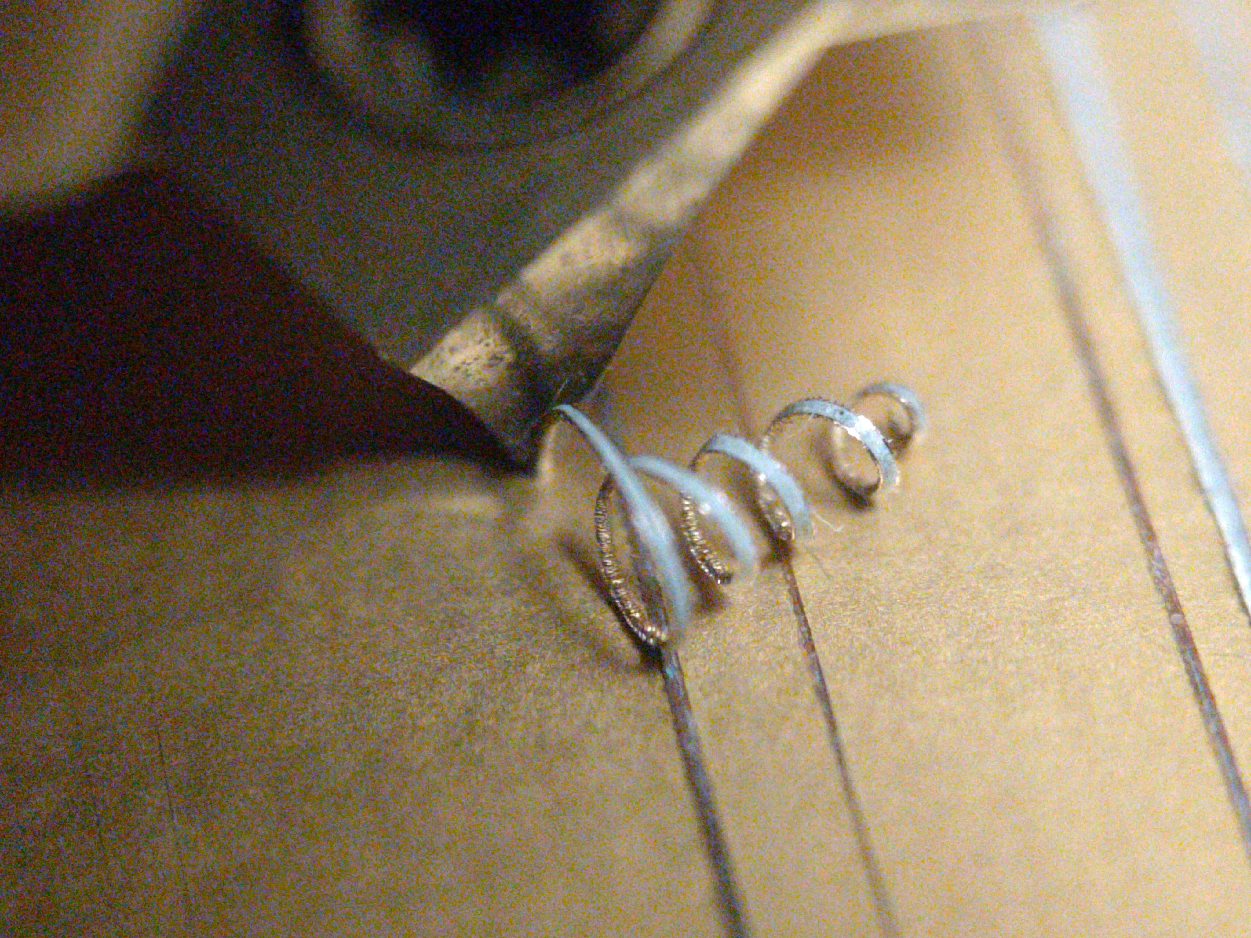
You could do this with a box-cutter blade, but that is not quite good enough for the resolution that [Zach] was hoping to achieve. To that end, he equipped the Circuit Graver with a carbide insert intended for use as lathe tooling. The tool has a 100 micron tip radius which can create a 0.2 mm trench in copper-clad board, right out of the box. That allows the creation of traces roughly around 8 mil or so. You can even sharpen the tooling and get it down to 0.1 mm or less, which is theoretically good enough for 4 mil spaces. That’s perfect for working with smaller feature size parts.
[Zach]’s talk provides a realistic assessment of the Circuit Graver’s real-world performance. Right now, it’s capable of carving 8/8 (0.2 mm) features on small boards quite well, while 6/6 (0.15 mm) features are “marginal.” The hope is to get down to 4/4 (0.1 mm) level with future upgrades. Speed is excellent, however—the Circuit Graver can carve good traces at 20-50 mm/s. For now, though, manual setup is still required—to ensure correct zeroing and that the tooling pressure is correct, for example.
It’s not something you’d use for production PCBs, per se—a real board house will always win for those sort of applications. However, for producing boards for quick prototyping, even with modern fine-featured components? It’s easy to see the value of the Circuit Graver. Imagine ordering some new parts and whipping up a unique project board just minutes or hours after you finish the design on your PC—it’s almost intoxicating to think about.
We actually featured the Circuit Graver on the blog last year—and there are design files on Hackaday.io for the curious. If you’re eager to start whipping up simple high-feature boards at home, it might be a build worth looking into!


That’s very cool.
As someone who has been frustrated by the realities of PCB milling for years, I’m open to any alternative that might actually be reliable. The pressure feedback part sounds very promising, since 70% of the problem with milling is the extreme sensitivity to Z variations. I do wonder how long the blades last, and whether they fail in board-ruining ways as they get dull; but replacing box-cutter blades is surely a lot cheaper and easier than replacing CNC cutters.
The slowness of milling is only like 5% of the problem, but faster is certainly better.
The other big problem is vias. This makes no difference on that front, but luckily I already found the solution, which is the teeny tiny 0.8mm copper rivets you can get from digikey et al. They might sound like a hassle but trust me, they’re far easier than all the horrible alternatives.
Pressure control as an option made a huge difference! I’m still interested in building a stiffer machine that perhaps could handle position control as a test, and I think there are interesting ways to loop-close that could make that feasible. Alternatively, it would be neat to automate pressure control; right now it’s a bit tedious to adjust, and often needs to be tweaked at the start of a job.
Despite finding the sharpest carbide turning insert I could source, I still ended up sharpening it a bit before use with a diamond-impregnated stone. No tip radius at all; bad for machining, but I never saw one crack. But to your point, I don’t think tool life is great, as I did end up re-sharpening the insert a few times. It’s hard to say how much this was needed, as other variables (see: manual pressure control) aren’t well-controlled, but if it was important then I probably sharpened after only a meter or two of trench production. Not great, but perhaps manageable with a built-in sharpening jig? Still not great.
Vias are certainly something I tossed into the “future work if ever” column. It’s a hard nut to crack. I’ve spent time with the little copper rivets you talk about and didn’t have a great experience; in my case, I had enough intermittent connections that I ended up chasing them all with flux and solder blobs, at which point I decided to just start using little bits of wire instead. In the circuit graver context, it’s all the more challenging since the machine doesn’t have a high speed rotary spindle, so adding a drilling operation isn’t just a trivial tool change.
Thanks for the comments!!
High speed steel takes a finer edge than carbide and may be more suitable for ultra-fine features.
Carbide is a cermet containing particles of some size and that means it will chip off in chunks at that scale perhaps.
If the work area were larger or more mobile, I think you could complete your entire process on one machine.
I would suggest an air spindle drill for its small size, just make sure it decouples the vibration expected in an air tool from the cutter itself.
Then add a wire feeder for the wire vias and a wiper on the bottom to flatten and a wiper instruction for the top with a shear attachment up against the wire feeder tip.
“since 70% of the problem with milling is the extreme sensitivity to Z variations.”
Yeah, we’ve got a high-end PCB mill in our lab (an LPKF ProtoMat) and they’ve got active Z-height maintenance to ensure depth cuts are precise. Plus micro end mills to cut flat rather than trapezoidally like a normal mill (which matters at GHz-ish frequencies, especially for coplanar structures).
Pretty sure they do it via pressure feedback as well.
Wow I’ve read about Protomats, they seem like wild machines. Granite plus 60k+ rpm spindles. My experience is only with hobby mills, e.g. Rolands, Carbides, Bantams, the like. How much is a Protomat? Does it get a lot of use?
Ours was 50k a number of years back. It got a bunch of use our first few years, but then drop ship cheap PCBs started getting faster and it dropped. We still use it for students a lot, though, and also RF stuff where we’ve got a stock of high performance dielectrics.
Software kinda sucks, of course. It should be able to do 2.5d milling, but haven’t been able to figure out easy software for that.
MITS (Japan) makes superb milling products. The application is a very quick learn. Double sided alignment is simple with a camera (no fixture pins). I have used several for 20+ years. Not cheap, true, but value.
The amount of experimentation this probably took to get right is beyond impressive.
Extraordinary work. I wonder if you could jerry-rig a blade like this on a Shopbot? I imagine it would require a LOT of tuning to do so, though.
I think the active rotary axis is important (vs drag knife mode), but that assumption should be pressure-tested! Could make a mean drop-in tool for a Zund, although those are harder to find vs shopbot-type routers.
This should be the future of home pcb, not fiber laser.