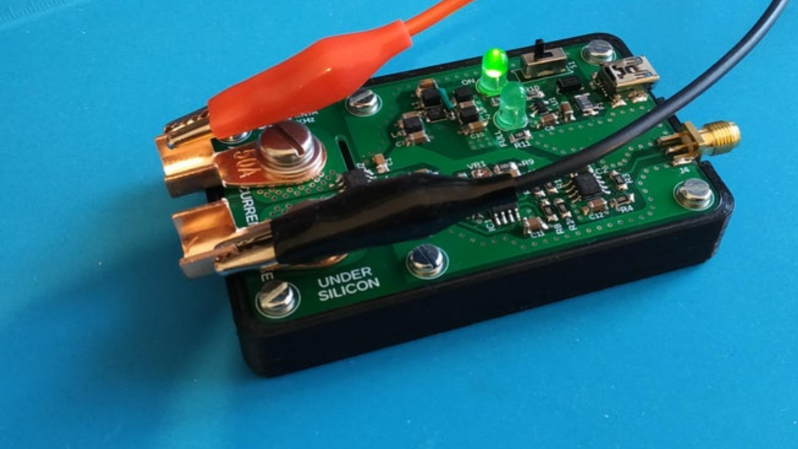
A decent current measurement sensor ought to be an essential part of every hacker’s workbench. One that is capable of measuring DC, as well as low and high frequencies with reasonable accuracy. And bonus credits if it can also withstand high bus voltages – such as those found in mains utility or electric vehicle work. [Undersilicon] couldn’t find one that ticked all the boxes, so he built an ACS730 based AC/DC current probe capable of measuring up to 25 A at frequencies up to 1 MHz.
Allegro Microsystems has a wide offering of current sensor IC’s. The ACS730 features a -3 dB bandwidth of 1 MHz, and -1 dB bandwidth of 500 kHz. Since it is galvanically isolated, it can be used in AC mains applications up to 297 Vrms and for DC up to 420 V. And as he intended to use it as an oscilloscope accessory, the analog output suited the application nicely. A pair of precision op-amps provide the voltage output scaled to 100 mV/A. The board is powered off a 1000 mAh LiPo battery that can run the sensor for about 15 ~ 20 hours. The power supply section consists of a charge circuit for the LiPo, and a split rail dual output power supply converter for the op-amps.
The ACS730 has a 2.5 V output when measured current is zero, and is scaled for 40 mV/A. This gives an output voltage swing from -0.5 V for -50 A to +4.5 V for +50 A. This is where the AD823ARZ dual 16 MHz, Rail-to-Rail FET Input Amplifiers step in. One pair is used to obtain a 2.5 V reference from the 5 V supply, and also to buffer the analog output from the ACS730. The second pair subtracts the 2.5 V offset, and applies a gain of 2.5 to get the 100 mV/A output. Dual power supply for the op-amps comes from a TPS65133 Split-Rail Converter, ±5V, 250mA Dual Output Power Supply. Lastly, LiPo charging is handled by the MCP73831 Single Cell, Li-Ion/Li-Polymer Charge Management Controller.


Initial testing of direct currents has shown fairly accurate performance. But he’s observed some noise when measuring currents below 1 A which requires some debugging to figure out the source. [Undersilicon] has provided the CAD files for both the PCB and 3D printed enclosure, giving you access to everything you need to build one yourself. If you’re looking for something a bit more heavy duty, you might be interested in this +/-50 A, 1.5 MHz sensor encased in concrete.


Nice one, thanks for posting :-)
Oh wow. Works just like my 50 mOhm brass bar.
Eek, you used to a live ‘earth’, your skin a silicon dioxide insulator ;-)
Is that the new “could’ve used a 555” but for measuring with scopes / shunts?
If so you won’t get too much isolation out of that setup…
bolt to plastic stand-offs
?
profit!
You’d be surprised how few analog isolation amplifiers there are, and they’re dog slow.
Si8920BD-IS for example has 0.1 MHz bandwidth. AMC1301 isn’t much better. differential probe circuits do higher bandwidth at the expense of true isolation and common-mode immunity.
Seems we’re stuck at the “?” stage here.
A few thoughts on the design:
* mains voltage and pollution degree 2 / 3 should motivate increasing clearance between the input nets and screws even though the assembly is probably intended to be put into a plastic enclosure. Allow for > 4 mm clearance.
* The outward-facing copper fill is superfluous, as it does not carry any meaningful current (export top Cu layer as .dxf and run a simulation in Agros2D or FEMM to quantify). It can be peeled back to improve clearance to the mounting hardware.
* I doubt the high current-side via stitching contributes in a meaningful manner. What’s more, It could make top layer sheet resistance worse and ultimately be detrimental. Via barrel resistance could be underestimated, bottom layer is unlikely to contribute to current handling capability in a way that justifies the construction.
* To improve top side current handling capability, strip-shaped openings in the stopmask are usually employed to add solder reinforcement of the tracks. I’ve also experimented with copper foil etched into segments for reinforcement. Others simply cut segments of Ag-plated Cu wire that is placed into strip-shaped overpasted “pads”.
* I’m not a fan of the single large via for high current contact mounting. WE RedCube terminals for example would be a perfect match for this application. They are available with M5 and M6 internal threads, like the press-fit version WP-BUTR (e.g. 7460305) or through-hole reflow version WP-WP-THRBU (e.g. 74655095). Rotate them 45° to maximize clearance and to get an even current distribution toward the sensor.
* I received a busted-up SMA to N – adapter the other day. SMA is rather fragile, and even though it might not look as nice, I think in this application something like TE 5-1634556-0 might work great.
Hi helge,
Thanks for the constructive feedback
I will take into account some of the things you have mentioned
Regards
You probably know this, but many do not. Spacing and material requirements have significant differences per the scope of the end-use equipment and the respective safety standard for the end-use construction and/or the standards scoped for the materials.
There are many standards that could be scoped; for example IEC62368-1, IEC61010-1, IEC60204-1, and UL508 off the top of my pointy evil mind. And the variations for the tabulations of spacings, test voltages, and materials limitations are significant for these standards
What a delicious idea. That sounds like a project that could have some commercial value once the bugs are ironed out., 👏
Certainly less expensive than Pearson current transformers. Looks good.
“You get what you pay for…”.
You can pry my two pearson CTs out of my cold, dead hands. The ACS ICs are not worthy of comparison to a good CT. And neither do LEM and Tamura current sensors have comparable performance to a good CT. The only advantage to Allegro, LEM, and Tamura stuff is that you can plant these components on a PCB.
The ACS devices are nice, but as Hall sensors are very noisy. They measure high current we’ll, but not low currents.. The opamps amplify and add noise. Would be better to create the math function in the scope…
The ACS730 is ridiculously sensitive to AC and DC external magnetic fields. Just changing the orientation in the ambient earth field can shift the measurement offset by several dozen mA. A quite small AC field (from, say, a nearby transformer or switching supply’s inductor…) will introduce its signal in the measurement too.
But you can negate the effect by using two devices back-to-back: just mount a second one in parallel, on the other side of the board, and measure the differential between the two device outputs.
You can also re-route the high current traces to put the two devices in series rather than parallel, thereby doubling your signal/halving the noise.
Thanks for the comment Paul,
The thing is, I do think that this type of ICs are not meant for measuring low currents at all, as they seem to work much better at higher ranges.
I designed the probe with high current power converters in mind, so the noise or the output not being precise in the tens of milliamps didn’t really bother me. However, I agree that there is still room for improvements.
Regards
Undersilicon
This is very nice.
Some scopes have active/FET probe jacks on them that’ll provide enough power to run the active probe; it’s possible you could use this to power the electronics in place of the battery. In some cases this is hidden behind an I2C identification, but in scopes from the ’90’s, it’s usually live power all the time.
Hi, thanks for the comment,
Yes, that would be a nice idea for a DIY project. But as you said, there is problably some shady protocol to hack in order to get power from the scope. And that would limit the probe to be compatible only with a certain brand of scopes I guess.
I only have a Hantek DSO5102P available in my workshop, so I designed the probe to be compatible with all the “less smart” scopes in the market like mine.
Regards
Undersilicon
[UnderSilicon]: Since you’re here, a couple of questions:
1. Why did you not use the VZCR zero-reference output? It appears not to be connected to anything except that 1 nF cap C2.
2. The VIOUT signal is going straight into the high impedance input of the opamp. Since it’s not loaded, VZCR is not loaded, and you’re not taking the difference between the two: How susceptible is this arrangement to capacitive coupling to the measurand side?
I’m just wondering how much spurious “current” you measure if you just have this connected in (say) a 60 Hz 120V hot line, from parasitic capacitance (a few pF at least) coupling that high side voltage to the 470-pF impedance input to IC1A.
Hi Paul, thanks for your comment,
Ups! My bad, maybe that could improve the noise problems. I take that into account for an improved version. Probably i wasn’t paying attention while reading the datasheet.
To be honest I think that is something that I would have to test in order to provide an adequate answer.
Regards.
Undersilicon
That looks nice (and useful)!
Regarding the noise at lower currents, maybe something like the ACS70331 is better suited? https://www.allegromicro.com/en/products/sense/current-sensor-ics/zero-to-fifty-amp-integrated-conductor-sensor-ics/acs70331
It is (or was last time i checked) available from Farnell for little money.
Hi,
That looks like a great idea for a low current version of the probe.
Also, this IC seems not to offer galvanic isolation. Only up to 100V, but still okey for non-isolated power converters I guess.
Regards
Undersilicon
Yes, i did not look at the isolation because i do not need it. There is probably a way to add some isolation in the “output path”, like some fancy linear isolation device if such things exists (??) or a differential scope probe or a isolated scope like those nice Fluke or…