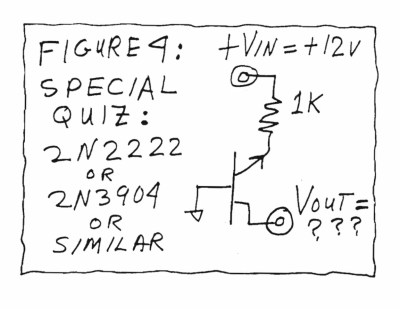
Back in 1996, Bob Pease posed an experiment in an April Fools column. “Take an ordinary NPN transistor, ground the base, pull the emitter up to 12 V with a 1 KΩ resistor and measure the collector voltage referenced to ground.” Do the experiment, and you might be surprised to find a small negative voltage present on the collector. [Filip Piorski] has always loved the riddle, and has explained how it works in a Youtube video.
 The key to the trick is the breakdown voltage of the transistor; normally somewhere around 7-8 volts for a typical small NPN transistor. At this point, where the base-emitter junction enters the breakdown regime, it begins to emit light. This light actually travels through the silicon lattice, where it reaches the base-collector junction, which acts like a photodiode under the right conditions. This generates the negative voltage seen at the collector under these conditions.
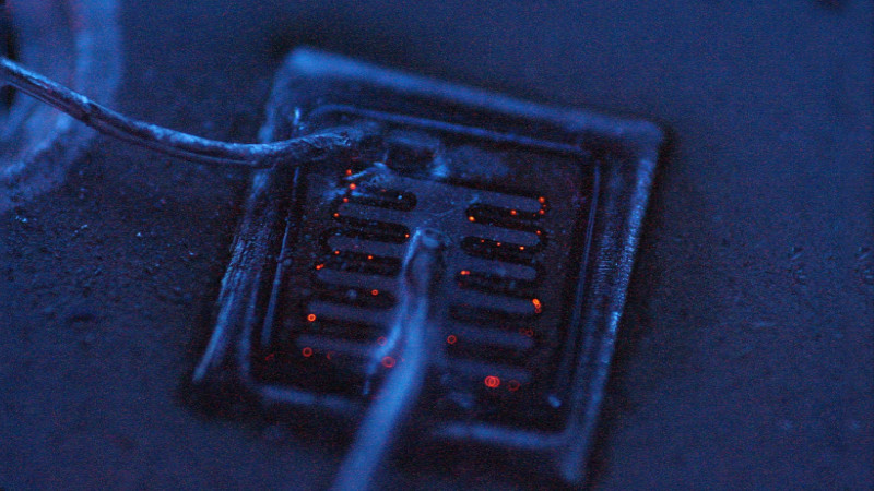
[Filip] goes on to try the experiment with a TO-3 transistor with the top cut off so he could visualise the effect in action. His photos, taken in a dark room, show tiny flecks of light appearing at spots on the silicon die. If you’ve got more insight on the effect in action, drop a comment below.
It might seem like a simple curiosity, however silicon junctions and their light emissions are an area of active research in semiconductor physics. Video after the break.


Back in the dark ages of CCD image sensors (eighties), it was common to find an odd elevation of signal in spots in a darkfield image. It’s supposed to be uniformly dark, with a bit of leakage current noise, but there were distinct regions near the edges of the sensors that had unusually high signal, like there were localized flaws. Or something almost like a small light source. For the most part it all came out in the wash after darkfield corrections, but it was a mystery.
It took what some thought an embarrassingly long time to realize that the hot spots corresponded to the locations of the output amplifiers, and a bit longer still to realize that the amplifiers themselves were emitting light, detected by pixels in the immediate vicinity. IIRC though, the light was infrared, not red.
Later CCDs were improved (geometry or process, I know not how), and the effect went away.
The issue was first observed in 1974 according to “6.2.12 Amplifier Luminescence” in “Scientific Charge-Coupled Devices”, James R. Janesick, 2001
I guess it just took a while for it to trickle down from The Father of the CCD to us plebes in the trenches. Nice to see he confirms my recollection though: the emission in this case is in the infrared.
CCDs have always been noisy. I had a Sony F828 back in the day. When you did long exposures with it at night. It would actually snap two pictures. 1st the actual picture, then a 2nd one of equally long exposure with the shutter closed. The camera would then internally subtract the nose from your image using the noise in the closed shutter image, then write out the final image to memory.
“CCDs have always been noisy. ”
Gee, that must be why they’re the weapon of choice for people who need professional-grade low-noise optical image sensors. :-/
The real answer is much more nuanced. Consumer-grade CMOS sensors are very good now, but used to be awful not very long ago. They have the advantage of being much more versatile and cheaper than CCDs, but pay a price in many other ways. But a good scientific-grade CCD will still blow away a CMOS sensor *for the application it’s designed for*. CCDs are just not as well suited for consumer-grade cameras.
A decent low-light CCD (like one I happen to have next to me here) has a dynamic range of 83 dB, a quantum efficiency of 96%, and a dark current (noise) equivalent of about 2 photons per square micron *per hour* — you can integrate for hours without the dark noise becoming significant. No CMOS sensor comes close. And much better CCDs than my (relatively) cheap one are available (for nosebleed prices, natch).
Your F828 was far from unique: most decent cameras did (and can still do) a dark frame subtract on long exposures. A modern camera is 100x less noisy though, so there’s less need for it.
We should try this with germanium transistors :-D
No, wasteful
i always thought it was an effect simillar to capacitive voltage doubling brought-on by rf reception providing the “clock” signal… or im just crazy.
im so glad to hear that there is a simple explanation.
PS: nice picture! i was never able to pop-the-top off of a 2n3055 myself…
I opened some 2N3055 decades ago, but only to observe the photodiode effect with external illumination. I would never have expected a (1) reverse biased) (2) silicon PN junction to be able to emit light.
The phenomena of semiconductor junction light emission inducing unwanted behavior with diodes, transistors and in-general ICs is a well studied subject.[1] Sometimes the emission wavelengths are in the human visual spectrum, often not. Photon-induced failures can be caused without on-die light emission, case in point: Photonic Reset Of The Raspberry Pi 2.[2]
^ References:
1. Light Emission | Semitracks
https://www.semitracks.com/reference-material/failure-and-yield-analysis/failure-analysis-die-level/light-emission.php
2. Photonic Reset Of The Raspberry Pi 2
https://hackaday.com/2015/02/08/photonic-reset-of-the-raspberry-pi-2/
What the actual heck!! That’s amazing!
I always assumed it would be some kind of electronic analogue of the Venturi effect or something.
So does this mean that Zener diodes are LED’s? With a different colour for each breakdown voltage?
I must try this tonight when it’s dark.
They will surely emit photons, though they may not be in the visible spectrum.
Cool Article – Thanx!