Imagine you’re sending a piece of hardware to space on a satellite. Unless you’re buddy-buddy with NASA, it’s pretty unlikely you’ll ever be able to head up there and fix something if it goes wrong once it’s launched. Robust design is key, so that even in the event of a failure in one component, the rest of the hardware can keep working.
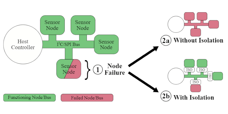
The problem is that these simple buses aren’t always the most robust, being vulnerable to single-point failures where one bad part takes down other parts of the bus. [Max] notes that vast numbers of sensors and devices rely on these standards, and it can be difficult or prohibitively expensive to design without them, so a solution was needed.
To fix this, [Max] developed a simple external circuit that could be placed on each node of a I2C or SPI communication bus. In the event of malfunction, that node can be cut off from the bus by this circuit, allowing the rest of the system to go on functioning.
With little more than a few transistors, MOSFETs and passives, you too could protect your buses from malfunctions using these techniques. [Max] did just that on the NASA V-R3x mission which flew successfully in January 2021 if you needed any further confirmation of the value of this technique.
It’s something that won’t bother the home hobbyist building a garage door opener, but it could be of great value to those designing systems that must fail gracefully if they fail at all. Be sure to share your best tips and tricks for robust SPI and I2C buses in the comments below!


Capacitance, capacitance, capacitance
Strong pull-ups, low clock rates.
Not sure I understand how this would help here. Since this is for the case when devices fail “on”.
Fworg64 suggested that the proposed solution will increase the parasitic capacitance of the bus. I suggested that stronger pull-ups will compensate and that lower clock rates make the limited slew rate less important.
I’ve also had it happen where I had too little capacitance (or too much inductance), and had to add decoupling capacitors at the end of long lines e.g. 6in jumper wires.
Seems like the kind of thing that should be made into an IC.
It is, but the part number starts with “LTC” so it’s a bit more expensive than a few transistors — but probably smaller. LTC4304
The IC likely isn’t space hardened either.
Not sure I understand how this would help here. Since this is for the case when devices fail “on”.
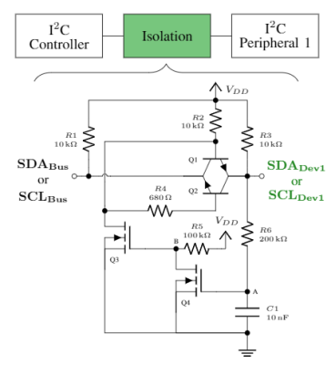
The bus is open collector pulled up, so “on” in this case means pulling the bus low.
In normal operation the capacitor charges up and pulling the bus low for brief periods of data transfer pulses doesn’t pull it down very far.
When a device fails “on”, it pulls the bus low. This eventually discharges the capacitor and locks Q1 and Q2 into high impedance, so the component pulling the bus low is effectively disconnected from the external bus.
If the device can fix itself and release the bus, the capacitor will eventually charge up again and the device will be reconnected to the system.
If you have N devices on the bus, the probability of failure is 1 – (1-P)**N where P is the probability of failure of one device. With lots of devices, this probability goes very high and a single failure would tank the entire bus.
The circuit shown can use components with a much higher reliability than the individual sensors.
“The circuit shown can use components with a much higher reliability than the individual sensors.”
this is what i’m struggling to understand. i guess i don’t understand what causes devices to fail in such a simplistic fashion. if it is so easy to avoid, why do the devices themselves remain susceptible to it? if devices tend to fail with a short to ground, wouldn’t that point to one or two transistors that tend to fail, and shouldn’t those be the focus instead?
it seems like we’ve simply moved the two failing transistors outside of the sensor, and i’m simply too naive to understand why that’s a win.
These sensors are usually complex IC’s – even full on microprocessors that communicate via SPI or I2C – any failure that breaks the whole bus rather than just making that sensors data garbage is going to be it asserting control and never letting go, which is what this is supposed to fix (and it might be doing that not for any failure of the sort you are talking about at all – if its had a bit flip that means its sending supposedly a billion times more than it should be it locks the bus up for ages, the data is garbage, but the communication is actually working as intended, and once its shifted through all the data/clockcycles it thinks its supposed to it will likely just work again).
It does nothing to make the sensor less failure prone in other ways, it just means if it fails in the way that prevents the rest of the bus from working it is disconnected. And being made of discreet larger gates its going to be much harder for outside radiation sources to cause that incorrect bit flip effect to break this and probably more temperature/impact/pressure stable too – where the dense little IC on the sensor board could get flipped with much less outside energy, borking the sensor at least till it hits some reset state.
Its a neat little circuit, wish I spent enough time with these sort of things to really just look at it and understand how it works from the diagram, but its not something I do much of, so when it comes up its always that puzzle to figure out how it works.
Why these devices sometimes fail is fairly immaterial, the fact is that it’s a not-uncommon phenomenon. Just search “I2C bus lock” and you’ll find countless examples. Oftentimes a low side NMOS
If we want to dig into this immaterial question, though,, an OTA update to the satellite could possibly command it to write an incorrect value to an address (no engineer is perfect), which if not protected for could lock up a device. Some ICs have been known to lock up under normal, correct use (no engineer is perfect). A marginally soldered pad could break free under the rigor of spaceflight, causing loss of or intermittent contact (no inspection is perfect). If this thing is in use for a long time (or sooner if some of the silicon is borderline), mosfet aging could happen in one of the ICs, causing a bus lock. Specifically to this use-case, they’re in space, and odds are many of these ICs aren’t space-hardened, so some radiation could flip a bit that would never be flipped under earthly operation (or at least many orders of magnitude less likely), and the device could lock up. Odds are, much of the IC count mentioned in the article is likely redundancy to protect for precisely this, so if your IMU gets wrecked by some radiation, or stops working for any other reason, you have 2 or 3 more that’ll let you keep flying. It’s likely that the bus’s master is also redundant.
The comment you replied to already went over the reason why it’s statistically very important to protect against this.
Could the same function be achieved with a single n channel fet, a capacitor and a resistor?
Connect the fet between bus and device, bus on the drain pin and device on the source pin. If the bus goes low, the fet acts as a diode and pulls the device low. If the device goes low and the gate is low, the fet remains off and the bus is unaffected. If the gate is high, the fet is on and the bus goes low too. Connect the gate to the capacitor as in the posted circuit.
Maybe this is a bad idea because of the relatively high capacitance on the gate, and having the whole fet move up and down with the signal is worse than the bjt transistors?
Not with a single n-fet as it needs to be bidirectional. Maybe with a n-fet and a p-fet in series but then you comes the voltage drop what makes it not suitable.
Fets act as a diode when reverse biased, though, and pulling the drain down on the bus side will cause the fet to turn and eliminate the diode voltage drop.
Here’s an ltspice simulation of what I’m thinking:
https://imgur.com/a/lnDJU2G
I added a diode to make the capacitor charge immediately on a high level. The core circuit consists of a 2N7002 N channel fet, a 200K resistor and 5nF capacitor (I misremembered, the original circuit uses 10nF), and a diode. There’s also the pull-up resistors of course. The rest of the components in the schematic are for generating test pulses. The first burst is bus side, the second burst is device side, and the last bit is the device going stuck low. The blue is device side voltage, and the green is bus side voltage.
It seems like it works? Maybe it’s too much capacitance though when you have dozens of them?
From what I can see it boils down to:
1) Can the I2C sensor properly drive the FET. (i.e. can it pull the FET high, could be solved with another pull up?)
2) When isolation is triggered, does bus voltage recover fast enough not to cause problems. (I don’t know enough about I2C)
A few couple more IC references for the same job:
ADuM1250/1
Si860x
The AD part works very well (and helps debug the bus if needed), I’ve done 550kbps over 50cm without any issues (over ethernet cable twisted pair.
The SiliconLabs part I never tested, but it’s (or was, I didn’t check prices) quite cheaper than the AD part.
NXP has some nice I2C interface parts. They do hubs, extenders and multiplexers. I would reach for the PCA9548A to do first simulations on. The author says “Products marketed as “digital isolator” or “hot-swap controller” might sound applicable, but these products do not pertain to fault isolation and would be unable to prevent a misbehaving signal from dominating the logic state of the bus [7].” I’m curious to what extent they looked into current parts – there are a significant number of sources listed in the paper.
Is this the simplest solution for open drain network?
I was thinking like a high pass filter that goes back to 0 on long DC.
So RC filter would do the same?
Check out my post above. I think the same behavior can be achieved with just a single n-fet, capacitor, resistor, a diode, and the two pull-ups. The diode is also optional but just seems like a good idea in either circuit, so apples to apples it’s 5 components vs. 11 components.
I’m not an EE, though, so maybe there’s a downside to my approach?
Designing for failure is a really difficult thing. The first question that came to mind was whether this additional circuitry is more likely to fail than the failure it is protecting against. Adding complexity is adding failure points and additional failure modalities.
If there’s a lot of other devices on the bus, then the increased failure chance is offset by the impact of a failure. Now there are more failures, but a failure will not take down the whole bus. Of course, more analysis would be needed to make sure that a single failure in the protection circuitry won’t take down the whole bus. Simplicity is the key.
Precisely, this looks to me like a much more robust circuit to keep the bus running than you would get in any IC, and should keep the bus running through any faults the other chips might throw, and from what I can see is very unlikely to fail in a way that does anything but disconnect an actually working device erroneously.
But I am far from a master of these sort of circuits, well outside my experience really. Which is why I always like reading these sort of articles, makes you think on something that really isn’t likely to ever apply to anything I do, but is well worth having an understanding of.
Kinda related: a friend pointed me at the LT1910, which is easily configured (as shown in datasheet) into a resetting solid state breaker with arbitrary (determined by value of current sense resistor) current range. It wouldn’t do well for a logic level problem, but it does quite well for individually isolating parts on a bus so that a short doesn’t crash everything.
I’m in the process of replacing the (terribly inadequate) fuse box on my vintage car with a design based on this, to individually fuse a dozen items that used to be covered by one fuse or nothing at all.
1- I think I2C is better than SPI for redundancy.
2- For critical system with many devices/sensors/actuators I might consider light as media.
3- Abother option is considering using de CS of SPI for enabling one circuits to manage each device (like example above).
“Quick and dirty” solution while also extending the BUS length/range, use Controllable (EN/DIS) Level Shifters for every device to lower the BUS voltage back to the same as the device uses which should allow for a lengthier BUS wiring while also enabling an easy way to isolate devices by disabling the Level Shifter.
Isn’t this exactly what you need? https://www.SparkFun.com/products/16740