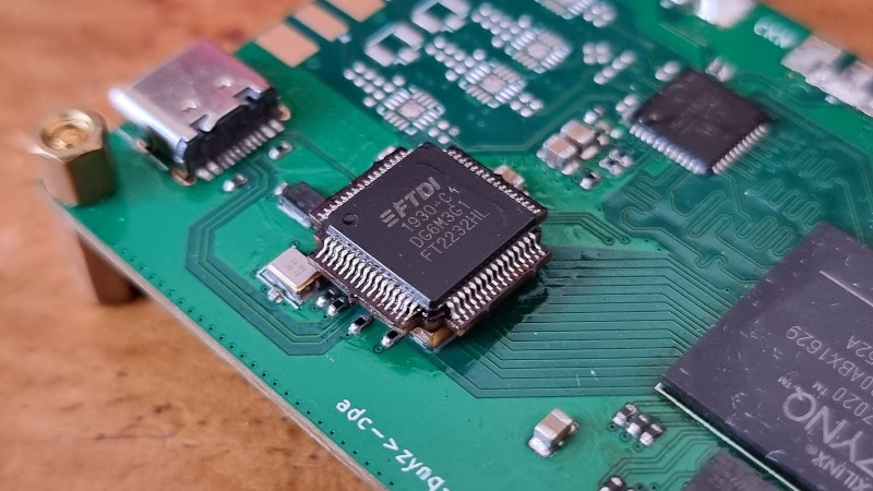
The semiconductor shortage has curtailed the choices available to designers and caused some inventive solutions to be found, but the one used by [djzc] is probably the most inventive we’ve yet seen. The footprint trap, when a board is designed for one footprint but shortages mean the part is only available in another, has caught out many an engineer this year. In this case an FTDI chip had been designed with a PCB footprint for a QFN package when the only chip to be found was a QFP from a breakout board.
For those unfamiliar with semiconductor packaging, a QFN and QFP share a very similar epoxy package, but the QFN has its pins on the underside flush with the epoxy and the QFP has them splayed out sideways. A QFP is relatively straightforward to hand-solder so it’s likely we’ll have seen more of them than QFNs on these pages.
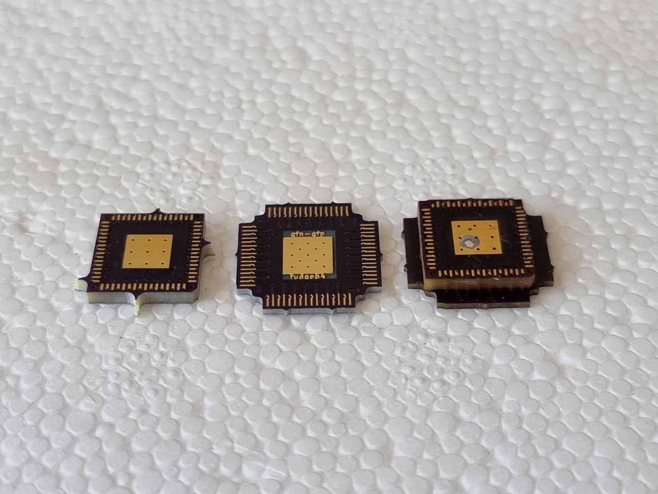
There is no chance for a QFP to be soldered directly to a QFN footprint, so what’s to be done? The solution is an extremely inventive one, a two-PCB sandwich bridging the two. A lower PCB is made of thick material and mirrors the QFN footprint above the level of the surrounding components, while the upper one has the QFN on its lower side and a QFP on its upper. When they are joined together they form an inverted top-hat structure with a QFN footprint below and a QFP footprint on top. Difficult to solder in place, but the result is a QFP footprint to which the chip can be attached. We like it, it’s much more elegant than elite dead-bug soldering!


Seems to me there coukd be a pin insertion made and then run the the wave to solder without liding control of the placement.
typo. oops. that would be ‘could’. And, I don’t know how there got to be two the’s! That would be ‘losing’ not liding. geez.
I thought the same solution to replace a fried QFP stm32f401 with a QFN version on my Nucleo 64.
A pox on FTDI.
Well, yeah, but are not the cause of the chip shortage.
No, indeed. They were the cause of “our driver bricks your (probably) counterfeit chip”.
Buy the legit chip instead of a slightly cheaper knock off and you won’t have a problem…leaching off someone else’s work is wrong.
The old sayings “you get what you pay for” and “play stupid games, win stupid prizes” seem to be apt.
Oh, hai. You must be new here. FTDI deliberately broke other people’s hardware. On purpose. How can anyone know what chips are embedded in every device? Yes, I’m a hot shot designer, and always buy legit stuff, but what they did was absolutely wrong, no doubt about it.
A pox on your house too. Kthxbye.
You’re assuming it was a conscious choice. Counterfeit chips are often sold as originals, at the same price. Sometime unscrupulous ODMs will substitute the cheaper parts, hoping you won’t notice.
Add some PTH in the center and it will be much easier to align with some short pins
You seem confused:
> a two-PCB sandwich bridging the two
> The three boards which make up the adapter
Looks like two is the correct number, with the picture showing (1), (2), and (1+2).
Well, five is right out.
HA! 3 being the number of the counting, the number shall be 3. 1-2-5 (three sir!)
2 + 2 is 4, minus 1 that’s 3
QUICK MAFFS
Is that something from Winnie the Pooh?
Monty Python and the Holy Grail
Book of Armaments
Boring, you should connect the two sandwich pcbs with bga balls ;-)
Good job!
You sir, are delightfully evil. :)
Improvise. Adapt. Overcome
We do these all the time to salvage legacy designs without having the expense to completely redesign / test and validate & qualify a released board. We refer to them as “Interposer Boards”. They are multi-layer, whereby use the original component footprint projected on the bottom side of the interposer, with the new package on the top side of the board. They are usually reflowed as a panel using higher-temp solder than the board it will be mated to. They can then be reflowed as a component in a typical SMT reflow
I use leadfree solder for the main reflow. 221C. So what do i need to buy that’s higher temp?
“ very similar epoxy package, but the QFN has its pins on the underside flush with the epoxy and the QFP has them splayed out sideways”
I do not have any at hand now to confirm, but, wouldn’t it be possible to bend the pins?
I wondered that too, turning it into some kind of J-lead package like PLCC, but very fine pitch. Seems like keeping the pins straight would be difficult – PLCC packages have little pockets molded into the bottom of the chip to help with this. QFN PCB footprint pads are tiny, not leaving much room for error or proper solder fillet to a lead. Might need to cut the QFP pins shorter as well.
Not sure about this FTDI part, but some devices in QFN/QFP don’t have exactly the same pinout. One example might be that the QFN die paddle is Vee/Vss/ground for everything, and what would otherwise be ground pins on the QFP version might be allocated for something else. Using an interposer gives you the opportunity to adjust the pinout if you can route the traces.
I’d love to see someone solder a J-lead modded QFP to a QFN footprint, that would be quite impressive!
The problem is that QFP leads tend to fairly brittle and require a lot of care and effort to get them bent correctly.
The QFN package for the same part is a lot smaller than the TQFP version. Look at the physical dimensions usually at the back of the datasheet. So even if you are able to fold the pins, the won’t make contacts with the pads.
I would have used the thinnest PCB or even a flex PCB for this task to make it easier to reflow.
Best practice is to design the board to accept multiple packages where possible.
Many industrial electronic products feature multiple footprints for various components.
It’s easy to be wise after the event.
This is something I wondered could be possible to upgrade flight controllers that aren’t supported by Betaflight anymore. Would be a fun project.
Seconded, adding “future proofing” to modern PCBs would make sense.