How Those NES DIP Chips Were Reduced To QFNs

The world of console modding leads us to some extremely impressive projects, and a recent one we featured of note was a portable NES produced by [Redherring32]. It was special because the original NES custom DIP chips had been sanded down to something like a surface-mount QFN package. Back when our colleague [Arya] wrote up the project there wasn’t much information, but since then the full details have been put up in a GitHub repository. Perhaps of most interest, it includes a full tutorial for the chip-sanding process.

To take irreplaceable classic chips and sand them down must take some guts, but the premise is a sound enough one. Inside a DIP package is a chip carrier and a web of contact strips that go to the pins, this process simply sands away the epoxy to expose those strips for new contacts. The result can then be reflowed as would happen with any QFN, and used in a new, smaller NES.

Along the way this provides a fascinating insight into DIP construction that most of us never see. If any of you have ever managed to fatigue a pin off a DIP, you’ll also no doubt be thinking how the technique could be used to reattach a conductor.

You can read our original coverage of the project here.

Nifty Chip Adapter Does The Impossible

The semiconductor shortage has curtailed the choices available to designers and caused some inventive solutions to be found, but the one used by [djzc] is probably the most inventive we’ve yet seen. The footprint trap, when a board is designed for one footprint but shortages mean the part is only available in another, has caught out many an engineer this year. In this case an FTDI chip had been designed with a PCB footprint for a QFN package when the only chip to be found was a QFP from a breakout board.

The three boards which make up the adaptor
The three boards which make up the adapter

For those unfamiliar with semiconductor packaging, a QFN and QFP share a very similar epoxy package, but the QFN has its pins on the underside flush with the epoxy and the QFP has them splayed out sideways. A QFP is relatively straightforward to hand-solder so it’s likely we’ll have seen more of them than QFNs on these pages.

There is no chance for a QFP to be soldered directly to a QFN footprint, so what’s to be done? The solution is an extremely inventive one, a two-PCB sandwich bridging the two. A lower PCB is made of thick material and mirrors the QFN footprint above the level of the surrounding components, while the upper one has the QFN on its lower side and a QFP on its upper. When they are joined together they form an inverted top-hat structure with a QFN footprint below and a QFP footprint on top. Difficult to solder in place, but the result is a QFP footprint to which the chip can be attached. We like it, it’s much more elegant than elite dead-bug soldering!

Flip Chips And Sunken Ships: Packaging Trick For Faster, Smaller Semiconductors

You may have heard the phrase “flip-chip” before: it’s a broad term referring to several integrated circuit packaging methods, the common thread being that the semiconductor die is flipped upside down so the active surface is closest to the PCB. As opposed to the more traditional method in which the IC is face-up and connected to the packaging with bond wires, this allows for ultimate packaging efficiency and impressive performance gains. We hear a lot about advances in the integrated circuits themselves, but the packages that carry them and the issues they solve — and sometimes create — get less exposure.

Cutaway view of traditional wire-bond BGA package. Image CC-BY-SA 4.0 @TubeTimeUS

Let’s have a look at why semiconductor manufacturers decided to turn things on their head, and see how radioactive solder and ancient Roman shipwrecks fit in.

Continue reading “Flip Chips And Sunken Ships: Packaging Trick For Faster, Smaller Semiconductors”

Fail Of The Week: When The Epoxy-Coated Chip Is Conductive

Every once in a while, you’ll find some weirdness that will send your head spinning. Most of the time you’ll chalk it up to a bad solder joint, some bad code, or just your own failings. This time it’s different. This is a story of weirdness that’s due entirely to a pin that shouldn’t be there. This is a package for an integrated circuit that has a pin zero.

The story begins with [Erich] building a few development boards for the Freescale Kinetis K20 FPGA. This is a USB-enabled microcontroller, and by all accounts, a worthwhile effort. So far, so good. The problem with the prototype boards was soon apparent. On some of the boards, the external 32 kHz oscillator was not starting. Resoldering the oscillator or microcontroller sometimes solved the problem, but not always. This is troubling, because that means the issue isn’t code, and it’s not the PCB. This is going to take a deep dive and a good inspection microscope.

One of [Erich]’s friends, [Christian B] somehow found the problem. When the Freescale K40 is manufactured, the die is carefully laid in a chip carrier and coated with epoxy, putting it in a small QFN package. The problem is, there’s an extra connection sticking out of one corner of this chip. This is just an artifact of the chip carrier, but if you leave exposed metal connected to ground, something is eventually going to go wrong.

The best guess [Erich] has is that this additional connection is from the manufacturing and packaging process, with the exposed metal pad in this application being bridged to an adjacent pad. Now, if there’s one failure to [Erich]’s design, it’s that the trace comes out of the pin on the adjacent pad at 90 degrees; this isn’t a best practice, but most of the time you can get away with it. This time, though, somebody got burned.

We don’t know how [Christian] ever found this issue. When you look at a tiny QFN package, you don’t expect there to be an extra pin attached to ground that can be easily bridged with a bit of solder paste. It’s either a lot of luck or skill to find this problem, but it’s a great example of the weird things you have to look out for.

Fail Of The Week: Marginally Documented Pad Shorts To Maskless PCB

[Erich Styger] was bit by a nasty gotcha when soldering a QFN surface mount chip. The problem rears its ugly head when combining a chip possessing a padless conductor and a PCB without a solder mask. As you can see in the image above, there is a conductor exiting the side of the plastic QFN, but there is no pad associated with it. For this reason, you won’t see the conductor documented in the datasheet as a pin. It is documented in the mechanical drawing of the package, without any explicit reference to its existence. This is the Jason Bourne of package quirks.

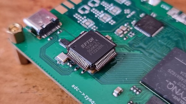
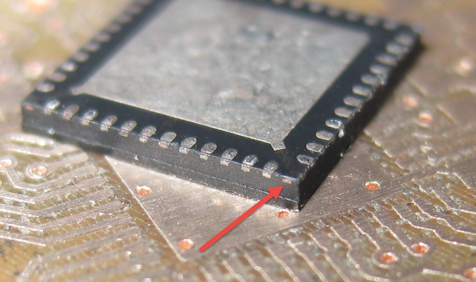
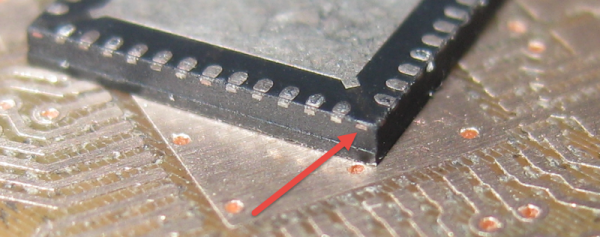
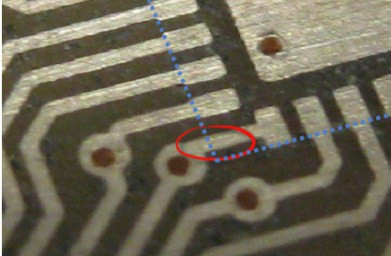
The PCB layout just happens to have a trace exiting right under this conductor. The two aren’t touching, but without solder mask, a bit of melted metal was able to mind the gap and connect the two conductors. [Eric] notes that although the non-pad isn’t documented, it’s easy to prove that it is connected to ground and was effectively pulling down the signal on that trace.

In a recent article on Hackaday I talked about “dangling pointers” and the challenge when interrupts expose the bug. [Erich’s] covered a ton of posts about embedded software. I was doing some poking around and was delighted to find that he covered the same concept and a solution for it using a program called cppcheck.

QFN Breakout Is Easy On The Eyes, Wallet

What do you do when you have ATMega328s in QFN package burning a hole in your bug box, but you aren’t set up for SMD and have limited access to parts? You man up and do what [Djpanjan] did: make your own breakout board with solder, right angle header, and many tiny, beautiful wires.

[Djpanjan] says the process is a simple one that requires great concentration. Once he had it broken out, he covered the wires with hot glue to make sure they all stay in place. He programmed it using an Arduino as an ISP and he was able to run the blink sketch without issue. He blinked all the output pins to make sure there were no shorts.

[Djpanjan] says that if he can’t get a breakout for his LQFP-144, he’s going to make his own again. Good luck, [Djpanjan]. We’re all counting on you.

If you’re set up for SMD and etching, there’s always the surface mount breakout route. If not, you can always use magnet wire and protoboard.

Shenzhen Tour And UnHuman Soldering Classes With DP

dp-hacker-camp

If you’re free the first week of April and don’t mind sitting on a plane for a looooong time you should check out the Hacker Camp that Dangerous Prototypes is planning. We’re sure you remember [Ian Lesnet] who is a Hackaday Alum, creator of the Bus Pirate, and geeky world traveler. Now’s your chance to try out what to him is a way of life.

The event is April 3-5 in Shenzhen, China. Although marketed as a “Hacker Camp”, to us it sounds more like training for those interested in running hardware companies that use the Shenzhen manufacturing district as the anchor of their supply chain. Part of the prep-work for the trip includes submitting board files which will be fabbed and ready for you on the first day. [Ian] and his crew will be your guides for the culture of the area; complete with meals and bar time. But there are also soldering workshops as part of the package. Don’t pooh-pooh the idea. This is unhuman soldering… BGA and QFN soldering instruction from the people who repair cellphones and other microelectronics.

This [Rick Steves] style adventure is the first that we remember hearing about that targets the open hardware community. But we must admit, it sounds like a lot more fun than a European river cruise!

[Thanks Akiba]