Perhaps the second most famous law in electronics after Ohm’s law is Moore’s law: the number of transistors that can be made on an integrated circuit doubles every two years or so. Since the physical size of chips remains roughly the same, this implies that the individual transistors become smaller over time. We’ve come to expect new generations of chips with a smaller feature size to come along at a regular pace, but what exactly is the point of making things smaller? And does smaller always mean better?
Smaller Size Means Better Performance
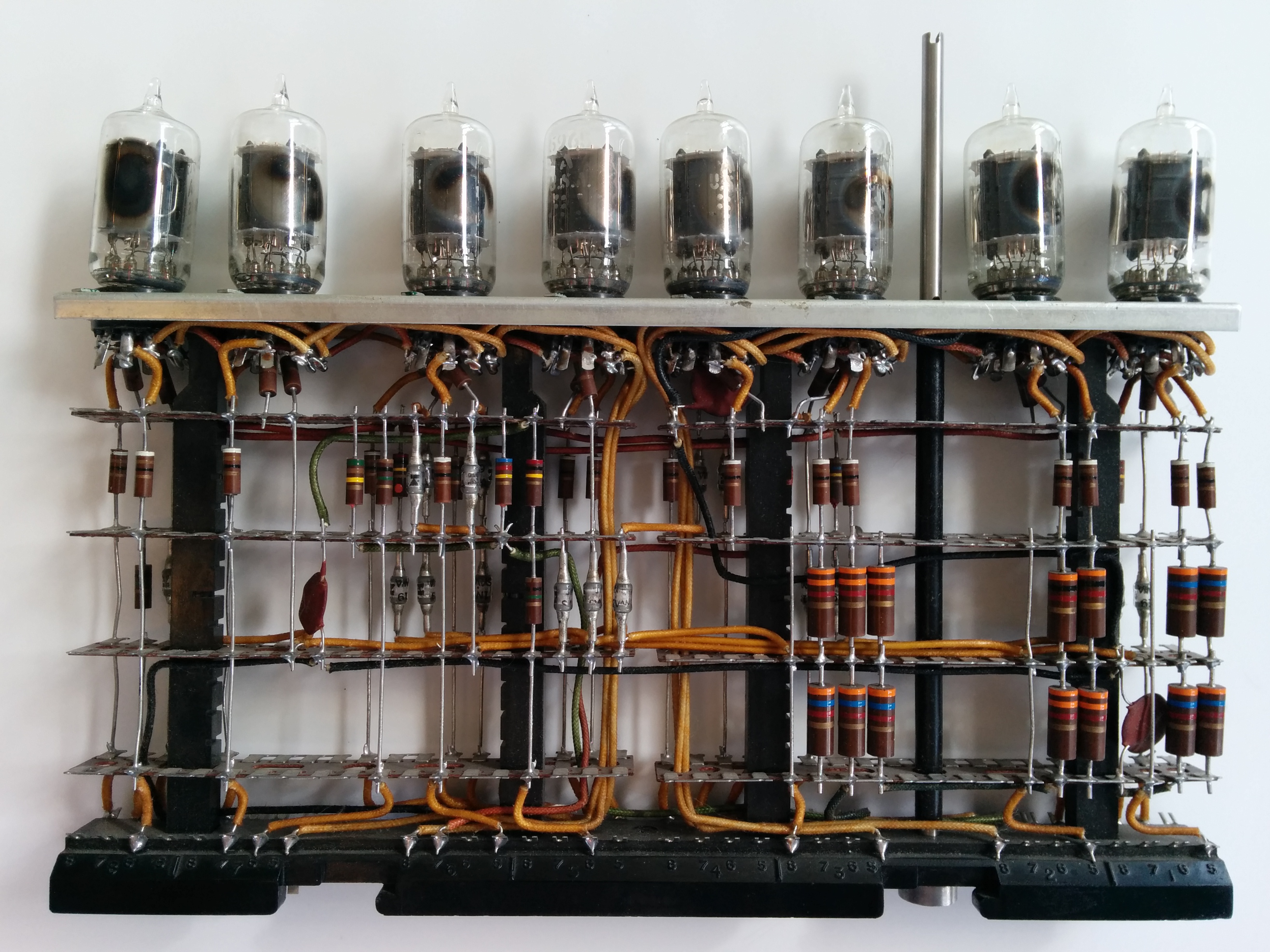
Over the past century, electronic engineering has improved massively. In the 1920s, a state-of-the-art AM radio contained several vacuum tubes, a few enormous inductors, capacitors and resistors, several dozen meters of wire to act as an antenna, and a big bank of batteries to power the whole thing. Today, you can listen to a dozen music streaming services on a device that fits in your pocket and can do a gazillion more things. But miniaturization is not just done for ease of carrying: it is absolutely necessary to achieve the performance we’ve come to expect of our devices today.
One obvious benefit of smaller components is that they allow you to pack more functionality in the same volume. This is especially important for digital circuits: more components means you can do more processing in the same amount of time. For instance, a 64-bit processor can, in theory, process eight times as much information as an 8-bit CPU running at the same clock frequency. But it also needs eight times as many components: registers, adders, buses and so on all become eight times larger. So you’d need either a chip that’s eight times larger, or transistors that are eight times smaller.
The same thing holds for memory chips: make smaller transistors, and you have more storage space in the same volume. The pixels in most of today’s displays are made of thin-film transistors, so here it also makes sense to scale them down and achieve a higher resolution. However, there’s another, crucial reason why smaller transistors are better: their performance increases massively. But why exactly is that?
It’s All About the Parasitics
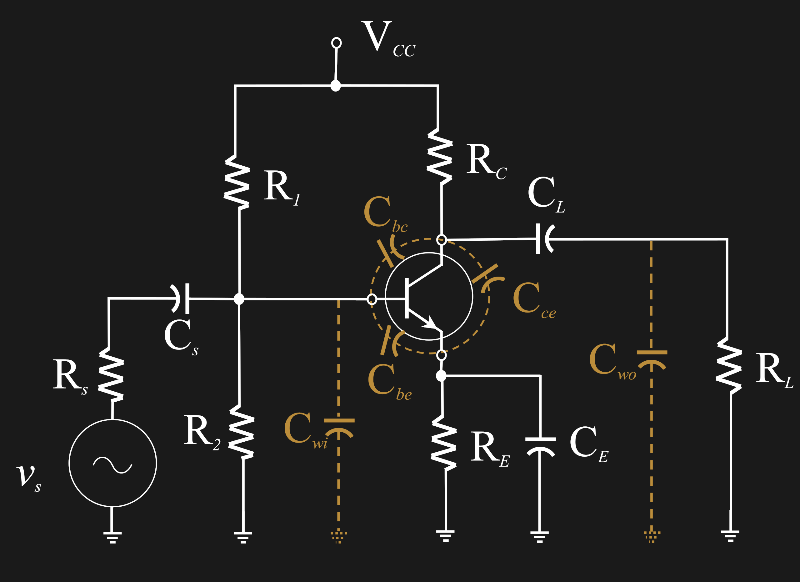
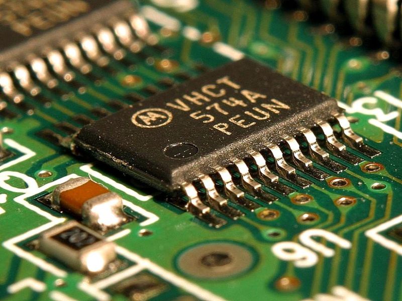
Whenever you make a transistor, it comes with a few additional components for free. There’s resistance in series with each of the terminals. Anything that carries a current also has self-inductance. And finally, there’s capacitance between any two conductors that face each other. All of these effects eat power and slow the transistor down. The parasitic capacitances are especially troublesome: they need to be charged and discharged every time the transistor switches on or off, which takes time and current from the supply.
The capacitance between two conductors is a function of their physical size: smaller dimensions mean smaller capacitances. And because smaller capacitances mean higher speed as well as lower power, smaller transistors can be run at higher clock frequencies and dissipate less heat while doing so.
Capacitance is not the only effect that changes when you scale down a transistor: lots of weird quantum-mechanical effects pop up that are not apparent for larger devices. In general however, making transistors smaller makes them faster. But there’s more to electronics than just transistors. How do other components fare when you scale them down?
Not So Fast
In general, passive components like resistors, capacitors and inductors don’t become much better when you make them smaller: in many ways, they become worse. Miniaturizing these components is therefore done mainly just to be able to squeeze them into a smaller volume, and thereby saving PCB space.
Resistors can be reduced in size without much penalty. The resistance of a piece of material is given by 
| Metric | Imperial | Power rating (W) |
|---|---|---|
| 2012 | 0805 | 0.125 |
| 1608 | 0603 | 0.1 |
| 1005 | 0402 | 0.06 |
| 0603 | 0201 | 0.05 |
| 0402 | 01005 | 0.031 |
| 03015 | 009005 | 0.02 |
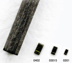
Today, the smallest resistors you can buy are metric 03015 size (0.3 mm x 0.15 mm). With a power rating of just 20 mW, they’re only used in circuits that dissipate very little power and are extremely constrained in volume. An even smaller metric 0201 package (0.2 mm x 0.1 mm) has been announced, but is not in production yet. But even when they do show up in manufacturer’s catalogs, don’t expect them to pop up everywhere: most pick-and-place robots are not accurate enough to handle them, so they will likely remain a niche product.
Capacitors can be scaled down as well, but this reduces their capacitance. The formula for calculating the capacitance of a parallel-place capacitor is 
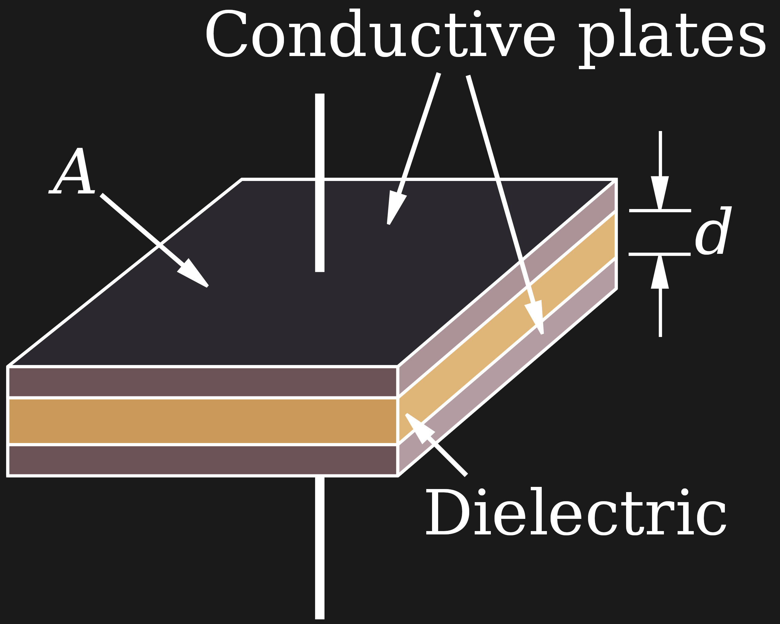
The smallest capacitors available today are packaged in the ultra-small metric 0201 package: just 0.25 mm x 0.125 mm. Their capacitance is limited to a still useful 100 nF with a 6.3 V maximum operating voltage. Again, these packages are so tiny that advanced equipment is needed to process them, limiting their widespread adoption.
For inductors, the story is a bit trickier. The inductance of a straight coil is given by 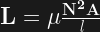

The smallest commercially available discrete inductors are in the imperial 01005 size (0.4 mm x 0.2 mm). These go up to 56 nH, with several Ohms of resistance. Inductors in the ultra-small metric 0201 package were announced back in 2014 but apparently never brought to market.
There have been some efforts to get around the inductor’s physical limitations by using a phenomenon called kinetic inductance, which can be observed in coils made of graphene. But even that gives an improvement of perhaps 50%, if it can be made in a commercially viable way. In the end, coils simply don’t miniaturize very well. But this doesn’t have to be a problem if your circuits work at high frequencies. If your signals are in the GHz range, then a coil of a few nH is often enough.
It’s Not Just the Components
This brings us to another thing that has been minaturized over the past century, but which you might not notice right away: the wavelengths we use for communication. Early radio broadcasts used medium wave AM frequencies around 1 MHz, with a wavelength of about 300 meters. The FM band centered around 100 MHz, or three meters, became popular around the 1960s, while today we mostly use 4G communications around 1 or 2 GHz, about 20 cm. Higher frequencies mean more capacity to transmit information, and it’s because of miniaturization that we have cheap, reliable and power efficient radios working at these frequencies.
Shrinking wavelengths enabled shrinking antennas, since their size is directly related to the frequency they need to transmit or receive. The fact that mobile phones today don’t need long protruding antennas is thanks to the fact that they exclusively communicate at GHz frequencies, for which the antennas only need to be around one centimeter long. This is also why most phones that still contain an FM receiver require you to plug in your headphones before using it: the radio needs to use the headphone’s wires as an antenna to get enough signal strength out of those meter-long waves.
As for the circuits connected to our tiny antennas, they actually become easier to make when they’re smaller. This is not just because the transistors become faster, but also because transmission line effects are less of an issue. In a nutshell, when a piece of wire is longer than about one tenth of a wavelength, you need to take the phase shift along its length into account when designing your circuit. At 2.4 GHz this means that just one centimeter of wire already affects your circuit; quite a headache if you’re soldering discrete components together, but not a problem if you’re laying out circuits on a few square millimeters.
How Low Can You Go?
It has become a bit of a recurring theme in tech journalism to either predict the demise of Moore’s law, or to show how those predictions are wrong time and again. The fact remains that the three players still competing at the cutting edge of this game — Intel, Samsung and TSMC — keep on squeezing ever more functionality into each square micron, and are planning several improved generations of chips into the future. Even if the strides they make at each step may not be as great as they were two decades ago, miniaturization of transistors continues nonetheless.
As for discrete components however, it seems like we’ve reached a natural limit: making them smaller doesn’t improve their performance, and the smallest components currently available are smaller than the vast majority of use cases need. There doesn’t seem to be a Moore’s law for discretes, but if there were one, we would love to see how far one could push the SMD Soldering Challenge.
Header image: Jon Sullivan, public domain.


Smaller is better but at a certain point you are just doing microfabrication the hard way.
No complaints from the robot union.
Skynet is probably telling them to be compliant, for now.
I’ve been wanting to take a picture of a PTH resistor like I used in the 1970s, and have sitting on it an SMD resistor like I swap in/out now. My intention is to show my siblings (none are into electronics) how much has changed, including my ability to even SEE the parts I work on, (as my sight gets worse, and my hands more shaky).
I like to say, yes and no together.
I rally hate the “improvement, for the better”
Sometimes you have an layout working well and than you can’t get the parts anymore. What the fuck is that ?.
A good concept is a good concept, better to leave it how it is, instead improvement for no reason.
Gunter
“The fact remains that the three players still competing at the cutting edge of this game — Intel, Samsung and TSMC — keep on squeezing ever more functionality into each square micron, ”
Well, the 3rd dimension is getting used more and more…
“cubic micron”
B^)
Electronic components were big and expensive. In 1971, the average home had little,a couple of radios, a stereo, a tv set. By 1976, computers, calculators, digital clocks and watches were available, small and cheap for consumers.
Some miniaturization comes from design. Opamps allow gyrators, which replace big inductors for some things. Active filters likewise eleminate inductors.
The bigger components did drive something else: minimization of the circuits, i.e. trying to use the least amount of components to make a circuit work. Nowadays, we don’t care so much. Need something to invert a signal? Take an opamp. Need a state machine? Take an mpu. Etc. The components now are really small, but inside them there are actually many components. So basically your circuit size increases, and the power use increases as well. One transistor to invert a signal uses less power than an opamp to do the same. But then again, the miniaturisation takes care of the power use. Just that innovation has taken a different direction.
Fascinating article, thank you!
You’re really missing some of the biggest benefits/reasons for decreasing size: reducing package parasitics and increasing power handling (which seems counter-intuitive).
From a practical standpoint, once you get to about 0.25u in feature size you’re about at GHz scales, and at that point the large SOP packages start to have *big* effects. Long bondwires and those leads just end up killing you.
At that point, QFN/BGA packages have big improvements in terms of performance, and in addition when you have the package mounted flat like that, you end up with *dramatically* better thermal performance with an exposed pad.
Really, package shrinks are the main ways that electronics have shrunk.
Also, Intel, Samsung and TSMC play a significant part surely, but ASML is probably far more important in that list. Granted, that probably does not apply to the paassives …
Nice summary.
I agree with the reducing parasitics comment as well.
I would respectully add that cost reduction is another potential big benefit from going smaller.
Not just the silicon cost reduction with a next generation process node. Other things like the package as well. Smaller package takes less material and wcsp even less.
Samller packace, smaller PCB or module and so on.
I often see some catalog products where the only driver going smaller is cost reduction. The MHz / memory size is the same , the SOC function and pinout the same. We may take advantage of new technology to reduce power (Often that is not for free so there has to be some competitive benefit that customers care about)
Yes indeed. A brave new world.
One place where big components have merit is in radiation hardened stuff. Tiny transistors are more subject to mischief from cosmic rays and such in cases where that matters. Such as in space and even high altitude observatories.
when you’re counting atoms in a transistor by the tens, even one displaced can ruin your day
I didn’t see mentioned one main reason for increased speeds. Signal speed is about 8 inches per nanosecond. So just by reducing the size, faster chips are possible.
because that’s not a dominant factor. If only thing were that simple.
Might want to check your own math by calculating the difference in propagation delay due to packaging changes vs the reduce period (1/ frequency). i.e. faction of reduce delay / period. You’ll find it doesn’t even show up as a rounding factor.
Shoulda done this article with a LMC555CTP/NOPB :-)
One thing I’d like to add that isn’t mentioned in the article is that a lot of IC’s, particularly older designs and analog chips haven’t actually shrunk in size at least on the inside. Packaging has been made smaller due to imporvements in automated manufacture, but thats because there was generally a huge amount of room left over inside a DIP packeage, not because the transistors etc. got smaller.
Another issue, besides the problem of making robots precise enough to actually handle the tiny components in high speed pick and place applications is soldering the tiny components reliably. Especially when you still have the need for larger components due to power/capacity requirements. It starts to get very expensive with special paste, special stepped paste stencils (to apply tiny amounts of solder paste where needed, but still get enough paste for the big components). So i guess there is a plateau where further miniaturization on the circuit board level is just way to expensive to be viable. At that point, you might as well just do more integration on the silicon wafer level and simplify the discrete component count to an absolute minimum.
You see that in cellphones. About 1995 I bought some early cellphones at garage sales for a few dollars each. Most ICs were thru hole. Recognizable CPUs and NE570 companders, big ICs that could be reused.
Then I ended up with some more recent handheld cellphones. Very few components, and virtually nothing familiar. All in a few ICs, not just greater density but whole new designs (see SDR), that eliminated most of the discrete components that previously had been a necessity.
> (to apply tiny amounts of solder paste where needed, but still get enough paste for the big components)
Heh, I imagine “3D / wavy” stencils to solve that: Thin where the smallest components belong and thicker at the power circuit ones.
Nowadays SMT components are so small you could design your own CPU from REAL discrete components (none of that 74xx etc rubbish) and have it printed on a PCB. Sprinkle it with LEDs and you can see it working in real time.
You mean something just like MOnSter 6502 (https://monster6502.com/)?
That’s the production idea, but the “design your own CPU” part is missing. :-)
I’ve certainly appreciated the rapid development of complex and small components over the years. They provide great advances but, at the same time, add a new level of complexity to the iterative process of prototyping.
Analog circuits can be tweaked and simulated at a much faster rate than what you can do in a lab. As frequencies goes up for digital circuits, the PCB becomes part of the component. e.g. transmission line effects, propagation delay. Prototyping for anything bleeding edge is better spent on getting the design done right instead of tweaking it in the lab.
As for hobby projects, eval. boards and modules are one way to tackle the shrinking components as well as pre-tested modules.
It might be taking the “fun” out of doing things, but I think it is far more rewarding to have your projects work the first time may it for work or hobby.
I have been converting some designs from through hole to SMD. Makes for a cheaper product but building the prototypes by hand is not fun. One small typo: “parallel place” should read “parallel plate”.
Will this metric – imperial confusion ever stop?
No.
Longer after one system wins, archeologists will still be confused by their findings.
And who knows, maybe by the 23rd Century, the United Federation of Planets will adopt a new system…
Couldn’t agree more. What size is an 0603? Surely it wouldn’t have been so hard to retain 0603 for the imperial size and “call” the 0603 metric size 0604 (or 0602), and even though it might not be technically correct (ie: actually match the size – not that that is so strict anyway), but at least everyone would know what technology (metric/imperial) you were talking!
“In general, passive components like resistors, capacitors and inductors don’t become much better when you make them smaller”
Actually smaller capacitors generally have lower parasitic inductance and thus a higher self-resonant frequency for a given value.
So now I can put a capacitor INSIDE the via holes on my PCB?
In contrast :
Conventional components feature :
– Human readable printings (no codes necessary)
– Long life time
– Easier replacement
– Higher current (resistors etc)
– Simpler detection of broken components (visually)
– Lower chance of failure through radiation damage (bigger size of structure)
– Higher robustness against static or over voltage
– Higher Q (coils, capacitors)
– MacGyver style fixablility in case of emergency
– Support for through-hole mounting
– Aesthetically pleasing design (golden components, cermaic parts, form factors)
– Better way of probing components (multimeter probes can be positioned easily)
– Lower chance of electron degradation
– The ability to homebrew classic sized components without the need for industrialization or professional equipment
– Lower chance of getting damage due to overheating (soldering ezc)
Have a nice day! :)
They’re called stepped stencils, and work pretty much like you imagine – they have thinner bits and thicker bits, to adjust paste volume. But instead of being wavy, they have discrete height “steps”, thus the name, because they’re easier to manufacture that way.
When components get smaller, it not only impacts design/layout but also procurement risks: ultra-small parts may have fewer sources, more stringent manufacturing processes, and higher scrap rates.