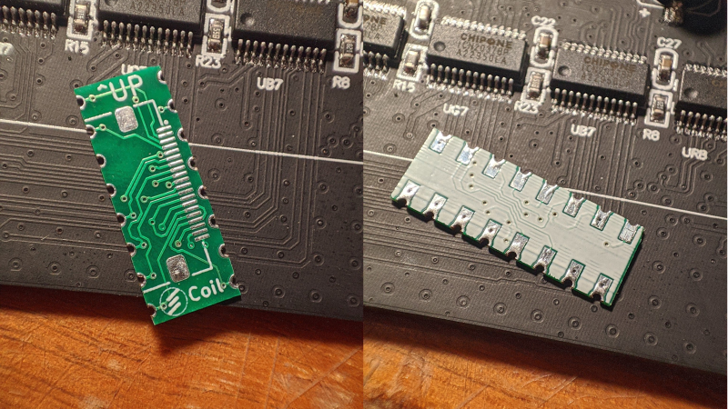
Castellated PCB edges are kind of magical. The plated semicircular features are a way to make a solid, low-profile connection from one board to another, and the way solder flows into them is deeply satisfying. But adding them to a PCB design isn’t always cheap. No worries there — you can make your own castellations with this quick and easy hack.
 [@CoilProtogen] doesn’t include much information in the Twitter thread about design details, but the pictures make it clear what the idea is here. OEM castellations are really just plated areas at the edge of a board that can be used to tack the board down to another one without any added hardware. The hack here is realizing that lining up a bunch of large-diameter vias and cleaving them in half with a sharp pair of scissors will result in the same profile without the added cost. The comments on the thread range from extolling the brilliance of this idea to cringing over the potential damage to the board, but [@CoilProtogen] insists that the 0.6-mm substrate cuts like butter. We’d worry that the plating on the vias would perhaps tear, but that seems not to be the case here.
The benefits of a zero-profile connection are pretty clear in this case, where castellated PCBs were used to replace bulky header-pin connectors on a larger PCB. We can see this technique being generally useful; we’ve seen them used to good effect before, and this is a technique we’ll keep in mind for later.


HEMIcírcular, not semicircular !!!
Bisected circular!
B^)
noun: hemicircle
a semicircular shape or structure.
Clearly it’s demicircular. See also how musical notes are divided into quavers, semiquavers, demisemiquavers, hemidemisemiquavers, semihemidemisemiquavers, and so on.
Do you even need castellations to connect one board on top of another? Just fill the vias with solder…
It’s hard to see if the joint is properly connected when filling vias as connections… Depending on your setup (reflow/hot air vs soldering iron), filling vias with solder can work. Castellations are pretty easy in comparison. I wouldn’t want to rely on filled vias with the tooling I have at home.
I also assume that desoldering it is easier with castellations instead of vias.
Just use a pice of bare wire through the vias and solder… done
Microstrip has an RF signal above a ground plane. stripline has the signal between two ground planes.
One double sided board, plus one single sided board, plus multiple connecting vias, equals… Stripline.
If you have SMT devices, you need to dril holes in the other board to get a flush mount.
I have done that with regular pads. Same trick as mounting SMT electrolytic caps, crystals. You just need slightly longer pads on the main board that are longer so that you can get heat and solder between the boards. It is doable for homebrew use.
It’s difficult to get the pads on the other board heated with a soldering iron. With notches both sets of pads can get heated at the same time.
What we’ve done at work is design a second set of vias on the lower board identical to the upper board, line them up, and stick long tail header pins through both for soldering.
With that said, save for very rare situations, I almost always want both top and bottom side components on boards since I’m more worried about board size than height. Our hardest packaging, LED drivers to fit in lightbulb bases, ended up using vaguely X-shaped boards to get the most stuff in the volume.
Scissors are a good way to make cracks in nearby traces. A shear is better, but still not great.
I use a belt sander. With a HEPA vacuum exhaust — that FR4 sawdust is nasty stuff.
What grade paper is on your sander? I ended up with a ragged edge on the through plating when I tried this with 100 grit. In some cases the through plating was pulled off completely.
I just use whatever is normally loaded: typically 220 garnet, but sometimes 120. The 80 grit aluminum oxide is definitely too coarse.
For a little board like this a jeweler’s saw would be reasonably quick. They’re a very precise way to chop up anything thin and hard.
Hang on… There’s a way other then this to do castellations?
This is a great idea for prototyping! I will probably try it myself. However, I would not do this for a production run of PCBs. Cutting the gold or HASL plating in this fashion will leave exposed copper which will oxidize over time and then eventually lead to failures. Applying extra solder on the finished joints by hand should be sufficient for prototyping though if care is taken.
Are you sure?
hemicylindrical
adjective. having the shape of half a cylinder (divided lengthways).
It is a 3D shape after all
Just make your boards with the spec to route out an area which takes away half a Plated Through Hole (PTH). That’s all a castellation is. You may get a sliver of hole plating left from the router bit on ende edge of the sliced PTH but you can trim those by hand or just solder them in when you solder the castellations. We’ve made thousands of boards this way fabbed by services like the purple board guys you already know at OSH Park. I’ll post a link to an example.
Do you have that example link?
Sanding to create castellations is easy by hand with 220 grit wet/dry sandpaper water flow. No dust. Solder wicking into via before cutting is also available. Less damaging. PCB is a wet process, so no possible damaging effects. but use distilled water to remove possible minerals if there is a concern. After solder attachment, wicking expoxy between boards will ensure permanent attachment. Chip attachment process used to secure LGA ( land grid array) packaged devices to normal production products, (under chip adhesive, reference Chip Scale Review magazine). Also used for high stress environments like CANNON LAUNCHED PROJECTILES (50,000 g’s shock). Used in Iraq 1991 by Hughes Aircraft Company supplier.