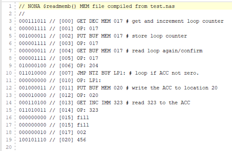
In the old days — we are talking like the 1960s and 1970s — computers were often built for very specific purposes using either discrete logic or “bit slice” chips. Either way, more bits meant more money so frequently these computers were made with just enough bits to meet a required precision. We don’t think that was what was on [Mad Ned’s] mind, though, when he decided to implement a 9-bit CPU called QIXOTE-1 on an FPGA.
Like many hobby projects, this one started with an FPGA board in search of a problem. At first, [Ned] had a plan to create a custom computer along with a custom language to then produce a video game. A quick search on the Internet led to that being a common enough project with one guy that we’ve talked about here on Hackaday before knocking it out of the park.
[Ned] then thought about just doing a no-software video game. Too late to be the first to do that. Not to be deterred, he decided to duplicate the PDP-8. Whoops. That’s been done before, too. Wanting something original, he finally decided on a custom CPU. Since bytes are usually — if not technically — 8 bits, this CPU calls its 9-bit words nonads and uses octal which maps nicely to three digits per nonad.
This first post talks about the story behind the CPU and gives a short overview of its capabilities, but we are waiting for future posts to show more of what’s behind the curtain in what [Ned] calls “Holy Nonads, Part 010.”
The downside to doing a custom CPU is you have to build your own tools. You can always, of course, duplicate something and steal your toolchain. Or go universal.


I once made a FPGA CPU using 18 bit opcodes, but still using a more traditional 32 bit data path. The 9th (or 18th) bit is a parity bit that comes free with the memory, allowing a nice addition to the opcode space.
See https://github.com/Arlet/x18-32
FPGA is never the answer.
FPGA is the answer for very specific applications, for example if you have a lot of data (as in, many gigabits per second) to move or manipulate with relatively simple operations.
Hey SparkyGSX! Nice to see you here. :-)
I was going to say the same, but had a different example in mind. Point remains: for specific cases, it can be very useful. One of the conditions is “low volume” when an ASIC doesn’t pay off. Sometimes the reconfigurability is important. And sometimes the we need some custom circuitry and too much of it to do with discrete LSI chips. (that’s how it started/grew from PALs and GALs).
The other use case is interfacing with custom ASICs. Old manufacturing processes are still useful in analog designs (you can easily do GHz stuff in quarter micron), so you do the analog in a custom ASIC and offload the digital stuff to an FPGA. Super common in scientific experiments.
Of course, Xilinx also now has chips which integrate ADCs/DACs which blow the cost/power ratios of discrete Gsps ADCs out of the water, so the use case for those is huge.
FPGAs have a few downsides compared to an ASIC.
Though, an FPGA also has a few upsides compared to an ASIC.
Depends on what one needs it for.
For very low volume applications where power efficiency isn’t a concern. Then FPGAs are actually rather decent, especially if one wants to fiddle with a lot of stuff in parallel, or use higher speed protocols that one typically won’t find elsewhere.
Though, the parallel nature of FPGAs can in a lot of applications just use a multi core microcontroller instead. Usually at a fraction of the price, and with superior power efficiency. But multi cored micros are usually a bit “odd” in their layout, making them at times a bit inept…
The high speed busses FPGAs offer is though typically not found on micros or even some SoC. So there FPGAs can be competitive if one only need a few hundred/thousand units.
If one however makes enough products, a dedicated ASIC will be more cost effective, if one can live up to a “few” requisites. Usually that one knows what one is going to need out of the chip, and that one doesn’t fudge up the design both from a logic standpoint, but also electrically (here FPGAs are pointless for simulation).
(Using an FPGA for logic simulation is this interesting thing that sometimes is super logical. And other times is pointless. Downsides with FPGAs as simulation tools is: 1. The design might not fit on the FPGA. 2. Routing out the design and pushing it over to the FPGA takes time, a software simulation has a decent head start. 3. Software simulation can log anything. 4. Software simulation can simulate the final chip on an electrical level if one has the tools.)
Though, we can peer into the auto industry and notice that even there FPGAs are used, despite sales figures in the hundreds of thousands, sometimes millions of units per year. So why aren’t they using ASICs one might ask? And the answer is reconfigurability, if one has made a mistake one can just fix it with the next firmware update. One don’t have to manufacture another ASIC and replace it in all units already sold. And this is a huge advantage for FPGAs.
But if power efficiency or peak performance are more important factors, and one is experienced in chip design, then an FPGA isn’t sometimes not even worth considering. (unless one can’t get access to a fab in time. Which is why some companies book their fab space before designing the chip.)
But in the end.
FPGAs usually gets glorified as this “magical silver bullet” that through some magical mean is supposed to have more performance, cost effectiveness and power efficiency than anything else. Even if it needs more transistor resources to be reconfigurable, adding both a higher power demand and larger latency into the logic, while also requiring a bigger chip with potentially lower yield. (not to mention that FPGAs also usually are stuffed with extra features one likely never will need.)
Though, if all one has access to is a 400nm fab, and the FPGA however is made at 22nm, then the FPGA might actually be better in all regards. As long as one don’t fiddle with purely analog/RF stuff…
But for the hobby bench, FPGAs are actually not that bad. (If it weren’t for the lack of easily acquired development tools for these chips…)
Luckily there’s a fully open-source toolchain that can generate bitstreams for some of the lighter Lattice offerings. Of course, generated bitstreams are not as performant as ones pushed by the OEM tools, but they aren’t the most performant FPGAs anyways.
The performance gap is closing. The open source tools are really developing. One vendor has already made them the official sw for their fpgas.
I worked on a commercial product with FPGA “glue logic” that actually turned out to be very useful, because we could upgrade the FPGA in the field too, and improve and rix the hardware remotely.
Agreed, it’s expensive, but sometimes you don’t have enough QTY to spin an inflexible ASIC.
We use them with great success in satellite modems. Unit cost is not very important, but the ability to upgrade the code is a big plus. For cost-sensitive products we do use a custom ASIC, as these are typically mass market things they would not be upgraded anyway.
“Since bytes are usually — if not technically — 8 bits, this CPU calls its 9-bit words nonads and uses octal which maps nicely to three digits per nonad.” is an interesting statement.
Though, usually a byte is just the smallest directly addressable unit in memory. (parity bits not included since they aren’t technically data.)
So if the processors smallest addressable unit is 9 bits, then its byte contains 9 bits.
There were also architectures that uses 4, 12, 16, 18, etc bits in their bytes.
This is supposedly one of the reasons network speeds are given in bits/second. Since bytes/second just didn’t make any sense. (Though, by the time the internet started becoming “common” I guess there were very very few systems in the world not using 8 bit as their smallest addressable unit. Though, some people might still be running some old 36 bit mainframe in their basement…)
Ahh, the good old days of yore, before the computing world settled on 8-bit bytes. Control Data was still producing CPUs with 60-bit words, each of which could hold ten 6-bit characters (or five 12-bit characters, if you wanted full upper & lower case support.) Since those machines were essentially hand-woven from discreet components, every extra bit and every extra word counted towards the price.
And the fun instruction set they supported was practically a national security issue. Those CPUs had a built-in instruction to count the number of “1” bits that were set in a register. This was an almost useless operation for the normal business and scientific computing of the era, but was a critical performance enhancement for code breaking.
That’s why I said “if not technically” and why network docs call them octets.
“Since bytes are usually — if not technically — 8 bits,”
Reading it aloud makes it sound like one concludes that a byte often is 8 bits long, and that one suspects it to be 8 bits by definition.
It feels like one of these observational statements, that adds in this “and that is likely a fact.” statements in a way that still makes a clear reservation for potentially being wrong.
And the thing that makes me look at it that way is because it continues in the same fashion.
“this CPU calls its 9-bit words [not bytes?] nonads and uses octal which maps nicely to three digits per nonad.”
(though, bytes and words are more or less interchangeable terms as far as architecture design goes… (I though prefer to always use Byte when it refers to the smallest addressable segment of memory. Though, this becomes interesting when most memory management systems handling cache tend to just work with whole cache lines instead… Sometimes to the point that memory allocation even works based on cache lines instead of bytes.))
If one however had written:
“A byte is usually 8 bits, but can technically be any number of bits long. This CPU have however gone with the name nonads instead for its 9 bit bytes. And it can neatly map 3 octals for each nonad.”
Then it would have been clear that a byte is just a name for a somewhat arbitrary unit in computing.
One could add why a byte isn’t always 8 bits, by just saying that “a byte is by definition the smallest addressable segment of memory, how many bits that exactly is becomes very architecture dependent.”
My car’s trunk-mounted CD changer apparently uses a 9-bit communication protocol…
Okay but the real question–and I can’t believe I’m the first person to ask this–can it run Eunux?
I believe the old HP41 calculators used 10 (ten) bit instructions.
IIRC the code, when released, used octal (1333) while enthusiasts used hexadecimal (244).
In order to handle 4 and 8 bit RGB values, I would probably look at 12 and 24 bit data values. But that’s just me.
Honeywell systems had either 8 bit or 9 bit bytes.