Thanks to the relatively recent rise of affordable board production services, many of the people reading Hackaday are just now learning the ropes of PCB design. For those still producing the FR4 equivalent of “Hello World”, it’s accomplishment enough that all the traces go where they’re supposed to. But eventually your designs will become more ambitious, and with this added complexity will naturally come new design considerations. For example, how do you keep a PCB from cooking itself in high current applications?
It’s this exact question that Mike Jouppi hoped to help answer when he hosted last week’s Hack Chat. It’s a topic he takes very seriously, enough that he actually started a company called Thermal Management LLC dedicated to helping engineers cope with PCB thermal design issues. He also chaired the development of IPC-2152, a standard for properly sizing board traces based on how much current they’ll need to carry. It isn’t the first standard that’s touched on the issue, but it’s certainly the most modern and comprehensive.
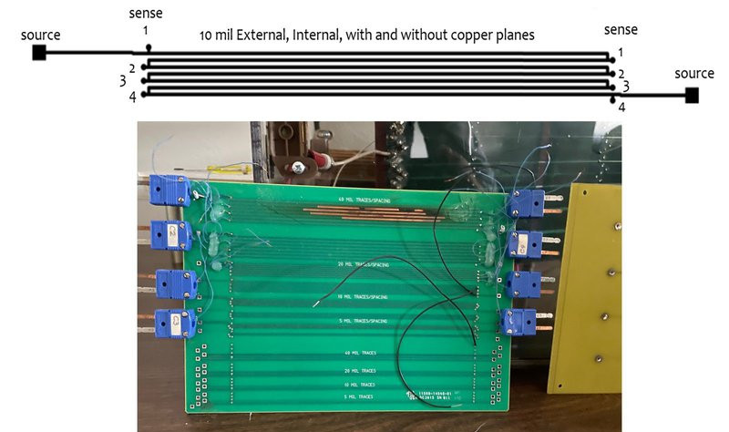
 It’s common for many designers, who can be referencing data that in some cases dates back to the 1950s, to simply oversize their traces out of caution. Often this is based on concepts that Mike says his research has found to be inaccurate, such as the assumption that the inner traces of a PCB tend to run hotter than those on the outside. The new standard is designed to help designers avoid these potential pitfalls, though he notes that it’s still an imperfect analog for the real-world; additional data such as mounting configuration needs to be taken into consideration to get a better idea of a board’s thermal properties.
Even with such a complex topic, there’s some tips that are widely applicable enough to keep in mind. Mike says the thermal properties of the substrate are always going to be poor compared to copper, so using internal copper planes can help conduct heat through the board. When dealing with SMD parts that produce a lot of heat, large copper plated vias can be used to create a parallel thermal path.
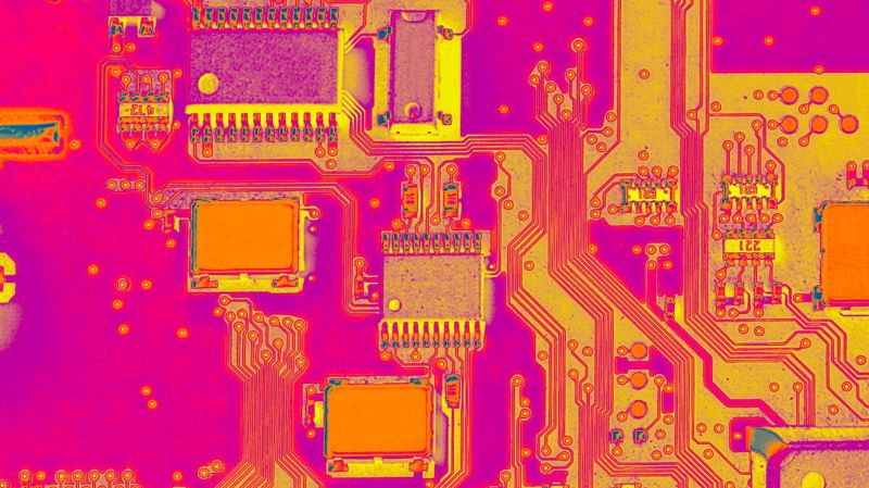
Towards the end of the Chat, Thomas Shaddack chimes in with an interesting idea: since the resistance of a trace will increase as it gets hotter, could this be used to determine the temperature of internal PCB traces that would otherwise be difficult to measure? Mike says the concept is sound, though if you wanted to get an accurate read, you’d need to know the nominal resistance of the trace to calibrate against. Certainly something to keep in mind for the future, especially if you don’t have a thermal camera that would let you peer into a PCB’s inner layers.

While the Hack Chats are often rather informal, we noticed some fairly pointed questions this time around. Clearly there were folks out there with very specific issues that needed some assistance. It can be difficult to address all the nuances of a complex problem in a public chat, so in a few cases we know Mike directly reached out to attendees so he could talk them through the issues one-on-one.
While we can’t always promise you’ll get that kind of personalized service, we think it’s a testament to the unique networking opportunities available to those who take part in the Hack Chat, and thank Mike for going that extra mile to make sure everyone’s questions were answered to the best of his ability.
The Hack Chat is a weekly online chat session hosted by leading experts from all corners of the hardware hacking universe. It’s a great way for hackers connect in a fun and informal way, but if you can’t make it live, these overview posts as well as the transcripts posted to Hackaday.io make sure you don’t miss out.


So the physics of the 1950s still hold true, but if you use lots of layers with large copper pours in between, the inner layers might not be more insulated. OK