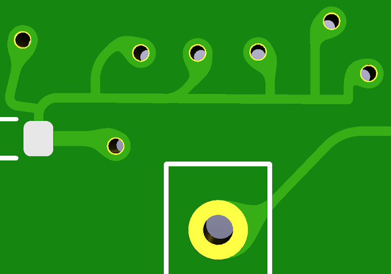
The first PCBs we built involved a draftsman laying out large pieces of tape. The finished artwork would be photographically reduced to produce the board. This solved a few problems. It was easier to work on the large pieces and any errors were reduced by the scale amount. Boards from this era have a distinct appearance because the tracks are generally curved. But when computer-aided drafting took over, the early packages couldn’t deal with wavy lines making all sorts of angles. So traces started appearing at very common angles like 45 degrees or 90 degrees only. If you use KiCAD, though, there’s no reason to have rectilinear traces. Now there is a plugin to help make your boards appear like old-fashioned circuit boards.
The video by [mitxela] below talks about how we got here and debunks some common myths about PCB design. The plugin produces rounded corners and teardrop-shaped pads. There’s also a second post on the topic with more details. The effect isn’t just ornamental. There are some reasons graceful traces might be better than sharp angles.


It is certainly not true that you can send “any design” and it will get “etched to perfection”. Even when I request electrical checks, I have received boards that turn out to have shorts. Making your design to reduce chance of errors is still a good idea. Nice rounded traces and teardrop pads are not bad of course, but I would still avoid sharp acute angles, especially when working at design limits.
Avoiding acid traps is quite important when pushing the capabilities of a PCB maker.
And it would be nice if KiCAD had an option to fail a DRC if an intersection creates an angle sharper than X degrees. (usually 90)
Likewise it would be nice if KiCAD had a tool that made angled corners of a specified size. (More or less just adds a triangle to said corner to ensure it is “always” less than 90 degrees.)
(maybe there is a plugin for this, but it really should be a feature of the base program…)
They are only a problem for home etched PCBs, you dont have to care about acid traps using modern manufacturing methods.
https://resources.pcb.cadence.com/blog/are-acid-traps-still-a-problem-for-pcbs-in-2019-2
Proof: look at any modern mainboard or other complex pcb, often they use grids as zone fill.
The only problem you have with home etched and square corners is that when your tinning the board the solder tends to pool in the corner.
I have also seen more de-laminations with square corners and cheap blanks.
The problem with that argument is that the smallest design features have decreased with the process improvements. When I started PCB design, it was normal to have 0.3 mm trace & clearance, and now I’m doing 0.1 mm.
Using grids as filler is not critical, because a small etching error does not compromise the electrical properties.
Yes. A lot of PCB manufacturers considers an 0603 resistor pad as somewhat large while the home etcher might consider it small.
One reason I did say “Avoiding acid traps is quite important when pushing the capabilities of a PCB maker.”
So if the PCB fabricator can etch 0.1mm wide traces, then having a sharp corner on such a trace isn’t ideal. But a similarly sharp corner on a 0.5mm wide trace on the same board it really doesn’t matter.
Or one might go to a cheaper manufacturer that is a bit more sloppy with etching, so suddenly one has to avoid acid traps on 0,5mm traces as well. It all depends on the capabilities of the manufacturer, but I rather avoid acid traps than buy a board that don’t end up working.
In my designs it’s not uncommon to find impedance controlled trace widths on the order of .03mm. We actually have custom tools at my work specifically designed to check for acute angles and we are expected to avoid them specifically so we don’t have any acid traps on our design. Fab processes have definitely improved but acid traps are still a very real aspect of board design in compact designs.
DRC checks for acid traps are already planned for development, but a detection algorithm is needed.
https://www.mail-archive.com/kicad-developers@lists.launchpad.net/msg38649.html
https://gitlab.com/kicad/code/kicad/-/issues/10580
What a clever and interesting chap!
I think a tool to make a PCB look like some Japanese calligraphy would be neat too. And for radio products do more inductors and capacitors as PCB art…..
Just a thought
Stephen G7VFY
I still design pcbs to maximise yield when things go wrong at the pcb maker i.e. being well more conservative than the pcb makers spec: thicker tracks, bigger spaces, oblique angles, fillets. The result are fewer rejects at every stage.
I would really like a tool that would thicken and spread tracks to use up the available space. e.g. if I design the pcb with 8 thou tracks and spaces as the pcb makers design rule, it jiggles them up until the free space is used up, or until they reach a target of (say) 15 thou tracks and spaces. Similarly ground and power nets would be jiggled to (say) 25 thou.
i remember using a built in tool in kicad 5 to thicken all traces on a board. it slows the pc to a crawl though, so you wouldn’t want fully automatic. it does save a lot of labour.
Yes, that would indeed be a nice feature, especially if you design power PCBs… ability to grow traces until the minimum gap is achieved rather than designing a PCB with a set track width.
Something similar is possible out of the box with pcb-rnd
http://repo.hu/cgi-bin/pool.cgi?project=pcb-rnd&cmd=show&node=routeradius
which is able to add a teardop to a padstack, and supports a bendy route radius mode.
Thinking about it, a custom padstack geometry with custom rotation per padstack instance might be a more elegant way of doing things.
gEDA PCB also supports teardrops, but does not have the bendy route radius capability, nor the custom padstack capability.
I just wanted to drop here to say this plugin looks awesome! I need to try it!
“The first PCBs we built involved a draftsman laying out large pieces of tape. The finished artwork would be photographically reduced to produce the board. This solved a few problems. It was easier to work on the large pieces and any errors were reduced by the scale amount.”
Can you clarify? Is that the royal “we”, because I don’t see reduction being necessary until ICs got small and tightly packed, and PCBs were around for a few decades prior. Though reduction probably first appeared in the medium scale integration era when semiconductor dies were mounted to circuit modules, 1960s?. Even in 70s and 80s PCBs were getting laid out at 1:1 for 8 bit computers and it has remained viable to this day for low density layouts. Just trying to illuminate the particular era referenced because the phrasing could be taken as meaning since PCBs first appeared they were photo reduced, which is not the case.
Layouts were done with flexible tape and donuts or pad patterns. The tape is kind of papery and flexible. It has an adhesive that does not dry so you can lift and lay again many times. You make curves by putting a finger on the tape move the roll around as you apply pressure and slide along. It works really well. Typically you use 2X or 4X on a big Mylar sheet. I have some on my wall as art. They are 4X and about 2 feet by 4 feet. You would have 3 or more widths of tape and a bunch of sheets with peel-off donuts and patterns. Section 2 here https://resources.altium.com/p/6-pcb-design-stats-to-make-you-look-smart-around-the-water-cooler
That adds precisely nothing to the understanding of when large scale masters became necessary and their particular application.
I see. Well, in case it wasn’t obvious, were are talking finger scale positioning limits and lining patterns up based on grid paper under the mylar on a light table. If you need 1/10 inch or better you have to work on scaled up art. They became necessary from the earliest use of DIP parts and particular of there will be machine insertion. But the process was used earlier. The printing industry used a “process camera” and Kodalith high contrast fine grained film to reduce art. The invention of the lithography offset press process spun off all the tools needed. About the same time that PCB’s became a thing, Joseph Gerber saw the coming calculator/computer revolution and moved his company away from the very clever calculating and drafting devices to a system and format for creating shapes and the optical aperture printers for them, which killed the taped art by the mid 1980’s
I’ll add my own testimony to this *very-clear* explanation. My experience is from the mid-1970s to mid 1980s. There was simply *no* physical means of laying out a PCB by hand without resorting to photographic reduction, including the layout of IC chip masks. In addition to PCBs, we laid out thick-film silk-screens the same way. Everything we did was at 6:1. We didn’t use blue and red tape. We used black “Chartpak” tape (similar in texture to masking tape) and a very sharp #16 Exacto blade to lay traces and donuts. Filleted donuts were available, but we didn’t use them. The draftsman had to be very careful in laying the tape. It had to be laid down with absolutely no stretching because it could then shrink back from the donuts over time (and largely undetected) leaving an open circuit. Though it would have been very useful to have whiteprints for (human eyeball) error checking, we were forbidden from running the layouts through the machine because its feed-rollers could move the tape around. I’m not exactly nostalgic for the whole process, but it had its charms.
70’s, 80’s and 90’s layout with tape at 2 or 4X was common. For DS boards we used red and blue Mylar tape on clear Mylar. Then photographic work could drop out the red and blue reductions separately to produce artwork to produce the PCB. In the later 90’s CAD packages became more common places. If you were working at 1:1 it would be almost impossible to run a trace between two pins on a DIP with the common pin spacing of .1.
This is cool. It does NOT look like old tape and donut design, which does not have the filleted joins of tape to circle. However, it resembles the hand-drawn layouts used in the lowest cost very high density boards for consumer electronics that used single sided boards. These had resistors mounted vertically and parts are pushed very tightly. They are a pain to figure out the schematic. https://www.ifixit.com/Teardown/Sony+TR-63+Transistor+Radio+Teardown/1219
I gave the plugin a try and was disappointed by my first test. I mostly use one layer for horizontal and another for vertical, and the plugin didn’t have much to say about those mostly straight connections between vias. I plan to try it again on some denser boards.
From a high-frequency signal-integrity standpoint, curved traces are better than sharp edges. I took a peek at the process, and well, it needs to be editable, and not a last-minute thing. It looks promising, though.
Rounded traces can be better than sharp corners, depending on the frequency you’re using.
I designed quite a few boards back in the day using velum Mylar and the requisite red, black, and blue tapes for double-sided boards. The boards I and my colleagues designed seldom if ever had curved traces, and at first glance they might pass as having been done in CAD. There were no 90-degree corners; when a sharp bend was necessary it was done in segments to avoid etchant traps. So no, curved traces and ‘tear-drop’ junctions with component pads were by no means universal.
Awesome!
I’ve always admired the Elektor Magazine board style. Any idea how they do that?
This article looks pretty wrong. This plugin is to improve manufacture. If you want to have curved tracks, to make them look more hand-made Kicad 6 has this feature built-in.
Quite a cool plugin for converting simple designs, one important thing to note is that track clearance rules are not followed so you may get a bizillion ERC error/warnings. This could be fixed in a hacky way by making the min. track clearance larger… but this means a less dense layout… With more development it has the potential to be an incredibly useful tool.