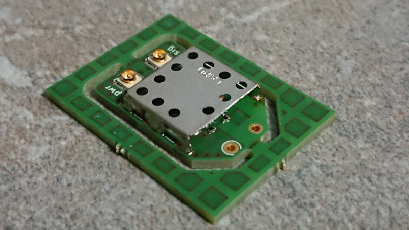
It’s a problem that has dogged electronic engineers since the first electrons were coaxed along a wire: that measuring instruments can themselves disrupt the operation of a circuit. Older multimeters for example had impedances low enough to pull resistor values, thus our multimeters today have high-impedance FET inputs. [Christoph] faced it with his oscilloscope probe, its input capacitance was high enough to put unacceptable load on a crystal oscillator and stop it oscillating. He thus built a FET input probe for higher RF frequencies, and its construction is an accessible view of wideband RF instrumentation design.
The circuit is a very simple one using a dual-gate FET, but the interest comes in the PCB and screening can design to ensure good RF performance. Off-the-shelf cans have four sides, so to accommodate the circuit one wall of the can had to be removed. The end result is a tiny PCB with miniature co-ax connectors for power and signal, which when characterised was found to have a 1.3 GHz bandwidth and a very low input capacitance.
If the language of RF design is foreign to you, may we recommend [Michael Ossmann]’s talk at a Superconference a few years ago.


Hmm, nice idea, I recall National Semiconductor had an application note some 25+ years ago for a 100MOhm diff amp with very cheap ICs, worked a treat though didn’t need it above a few 100KHz. This one might well open up a new possibility which wasn’t feasible back then, thanks for posting, nicely done :-)
I once had the same need to measure some stuff with a low capacitance probe. Been on the cheap I went to the big auction web page and found a “RF Active Probe 0.1 – 1500 MHz – 1.5 GHz Analyzer Oszilloskop” that is essential the same design around a BF998 from an Ukraine seller. It looks home made and was of middle quality but enough for a cheapo like me.
It works great.
Just saying.
Well, most of us have low-bandwidth scopes anyway, so a DC-300MHz FET probe would be better suited for looking at crystal oscillators, opamp inputs and e-fields.
Quick tip: run a trace from the input cable’s shield to a guard ring around the jfet’s gate, then connect it to the output.
It’s called ‘bootstrapping the cable’. It reduces the effective input capacitance by holding the voltage between the signal line and the nearest conductor more or less constant. If there’s no change in voltage between the plates of a parasitic capacitor, the signal doesn’t lose energy charging or discharging that capacitor.
In practical terms it just shifts the capacitance issues out a layer. Instead of losing energy from the signal to the shield, you lose energy from the shield to GND. The shield’s energy comes from the low-impedance output though, which is much better equipped to handle the load.
As is so often the case, Jim Williams described it in a Linear App Note:
https://www.analog.com/media/en/technical-documentation/application-notes/an21f.pdf
Damn good point mike stone And thanks for the link, if at least to clarify with more detail and also for some to converge on correct interpretation too :-)
Bootstrapping cables at up to 1.3GHz ? Not really … Except you want to build an oscillator :)
Too bad that BF998 dual-gate FET is unobtainium now. It’s a pretty neat device. I got some of the very last ones Digikey sold, in 2014 (!). I’m guessing there some NOS laying around, and there are some kinda-work-alikes, but that one device was nearly unique in its characteristics.
What I see eBay and others have plenty of stock left, so no concern for hobbyists. Still looking for a replacement …