What do you get when you cross a modern super-scalar out-of-order CPU core with more traditional microcontroller aspects such as no virtual memory, no memory cache, and no DDR or PCIe controllers? You get the Tesla Dojo, which Chips and Cheese recently did a deep dive on.
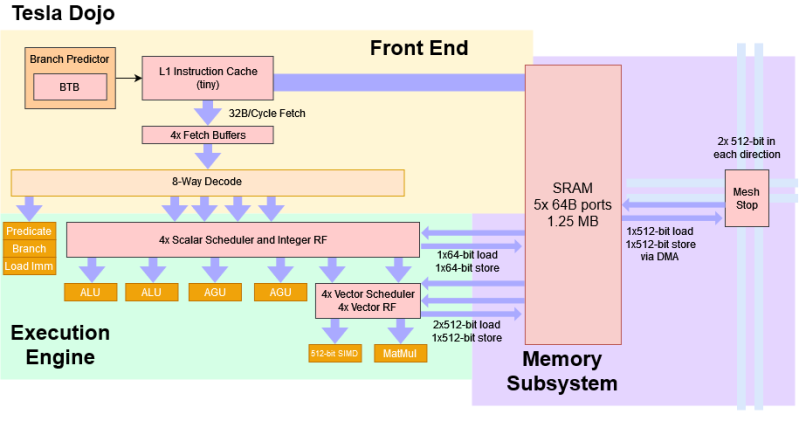
It starts with a comparison to the IBM Cell processors. The Cell of the mid-2000s featured something called the SPE (Synergistic Processing Elements). They were smaller cores focused on vector processing or other specialized types of workloads. They didn’t access the main memory and had to be given tasks by the fully featured CPU. Dojo has 1.25MB of SRAM that it can use as working memory with five ports, but it has no cache or virtual memory. It uses DMA to get the information it needs via a mesh system. The front end pulls RISC-V-like (heavily MIPS-inspired) instructions into a small instruction cache and decodes eight instructions per cycle.
Interestingly, the front end aggressively prunes instructions such as jumps or conditionals. However, eliminated instructions aren’t tracked through the pipeline. Instructions are not tracked through retirement, so during exceptions and debugging, and it’s unclear what the faulting instruction was as instructions are retired out of order.
Despite the wide front end, there are just two ALUs and two AGUs. This makes sense as the focus of integer execution is primarily focused on control flow and logic. The actual computing horsepower is the vector and matrix execution pipelines. With 512-bit vectors and 8x8x4 matrices, each dojo core comes close to a full BF16 TFLOP. The result is something that looks more like a microprocessor but is wide like a modern desktop CPU.
All these decisions might seem strange until you step back and look at what Tesla is trying to accomplish. They’re going for the smallest possible core to fit as many cores on the die as possible. Without a cache, you don’t need any snoop filters or tags in memory to maintain coherency. On TSMC’s 7nm process, the Dojo core and SRAM fit in 1.1 square millimeters. Over 71.1% of the die is spent on cores and SRAM (compared to 56% of the AMD Zeppelin). A single Dojo D1 die has 354 Dojo cores. As you can imagine, a Dojo die must communicate with an interface processor, which connects to the host computer via PCIe. However, Dojo deployments often have 25 dies, making this a very scalable supercomputer.
If you’re curious about peeling back the layers of more compute cores, look into Alder Lake.


Dojo* arigato mister roboto
Great classic album!
FP16 or BF16 Throughput: 362 TFLOPS
That means that each of the 354 cores (clocked at 2GHz) has the potential to do about 512 16-bit floating point operations every clock cycle.
Vector FP32 Throughput: 22 TFLOPS
That means that each of the 354 cores (clocked at 2GHz) has the potential to do about 32 32-bit floating point operations every clock cycle.
That is totally insane performance. And at 600W makes the car nice and warm in the winter time :)
600 watts is substantial – especially when driving at city speeds (say 12 mph average), that makes the computer be 20% of all the energy required for driving.
I wonder if future car instructions will say “drive on manual to save energy”.
These are for training the AI model not for the car.
Compute could be “free” during the winter if the heat could be dumped into the cabin.
These aren’t for cars, they’re for data centers.
No cache, no virtual memory, and some big ol’ vector units. It’s like it’s 1989 again and Crays are roaming the earth. Excellent!
exactly ;)
Is it available in mass-produced hardware? Or is like their famous battery-swapping, cybertruck, humanoid robot, actual full self driving, robotaxis, etc?
Check out Anastascia’s review. This isnt for in the car and at the moment its for in house use only. They are replacing all the NVidia AI units in their learning environment with these. Hence tyhe Name DoJo.
If they’re smart, they’ll open them up for everyone else to use too – as well as being a great revenue opportunity, if an ecosystem is built around this hardware, it’ll help them with hiring.
Oh well…….
Soon Tesla will own the self-driving space.
And with the brain interface, they’ll own much more!
Always soon, always mere 6 months away. Like robotaxis.
Sorry I don’t get dojo meaning
Dojo? The name of the martial arts training location, specifically Karate but often used across different styles and forms?
BF26 ? What’s that beast ?
It´s the typo beast biting the lazy writer of flop articles.
They meant BF16. https://en.wikipedia.org/wiki/Bfloat16_floating-point_format
I prefer rather Epiphany Parallela 1024 or more, because communications is faster then here
trouble is no new CPU on market
The issue was the author started working for DARPA ;)
How do that manage to not saturate the IO bandwidth with that level of computing power?
I remember when Google showed some early info of the TPU, it had issues with some models because it basically got IO bound.
That’s the $Billion question. They must be putting a ton of work into the software controlling DMA.
Reminds me of the Parallella chips.. architecture is same grid like structure of simple mcu like cores.
How is 1.25 MB of local SRAM not a cache? This just sounds like semantics to me.
Is there some special property of a cache I’m not aware of? And no I don’t mean “how caches usually look”, or “in this case the processor has to populate the cache, not the mmu”. That’s just a shell game moving the work around.
It means all your pointers will be 24 bits instead of 64 BITS(48 effective) , because if you access something outside your 1.25MB SRAM address space, you’ll segfault. No VM, and no snooping. DMA is OS level big block transfers – not little 64 byte cache lines. This is optimized for highly parallel fixed sized blocks of memory where some pre and post code DMA the source in then DMA the computed answer out (namely a 1MB texture and a 256KB weights array (that is being successively refined). You keep copying in your grays scale 1024×1024 textures – round robined through each core on the DMA, and after 1 million rounds you copy the weights file out (over DMA).
In a GPU, you would have to copy in the textures over a PCI bus (because you can’t have 50TB of training data in GPU RAM. And that same bus would have to feed 64byte cache lines to each SMP.
In CPU, every 64byte read has to stall the L2 cache lines of the peers (which practically limits max NUMA sizes). In xenons and ARMs you CAN have cache NUMA groups, but it complicates scale out algorithms (think having micro docker containers vs one MASSIVE suite of threads.) but every VM load has a TLB miss cost, and a multi hundred ns shared DRAM load. In theory, this style avoids those choke points. (but requires a completely different software stack)
Connection machine?