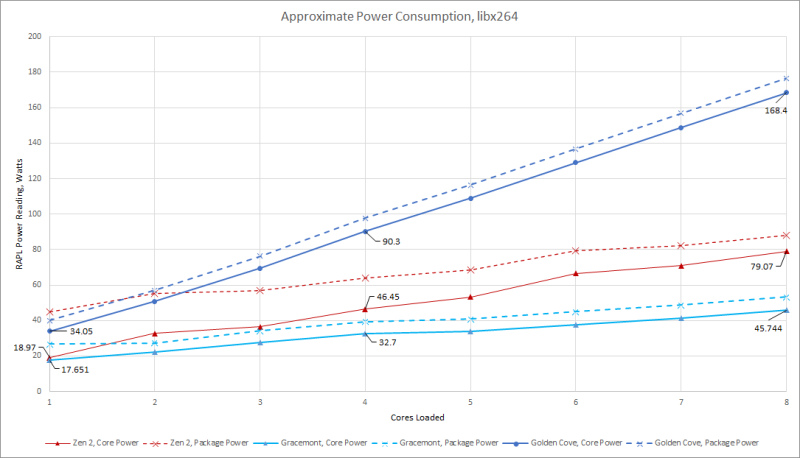
The winds of change are in the air for CPUs. Intel has long lorded over the computing world, and they remain a force to contend with, but many challengers gather at their gates. AMD, ARM, IBM, and other X86 designs sense a moment of weakness. In response, Intel released their Alder Lake platform with high-performance and high-efficiency cores, known as Golden Cove and Gracemont, respectively. [Clamchowder] and [cheese] have written up as many details as they were able to suss out about Gracemont.
ARM has done a multi-multi core design (big.LITTLE) for several years where they have a mix of high-power, high-performance cores and smaller, low-power cores. This allows the scheduler to make tradeoffs between power and performance. Typically the smaller cores in an ARM design are simpler in-order processors, having more in common with a microcontroller than with a full-scale desktop core. Many people have made an obvious comparison with the apparent similarities between ARM’s approach and Intel’s new offerings as Gracemont is based on Intel’s old Atom core, a low-power single issue, in-order processor.
[Clamchowder] and [cheese] were able to demonstrate that the Gracemont core in Alder Lake is nothing like Atoms of old or the tiny processors in ARM’s big.LITTLE. It is a multi-fetch, multi-issue, out-of-order processor. Given that it is so similar to the much more powerful Golden Cove processor, it gives us the chance to look into Intel’s tradeoffs to make a higher efficiency core. All of this information comes from significant guesswork and testing, slowly zeroing in on the sizes of different caches and the architecture of the branch prediction system.
It’s a fascinating read on the interworkings of a chip with real attention to detail. But, if you’re interested in peering even deeper, we covered extracting an actual gate from a processor.
Thanks [Carson Bunker] for sending this one in!


It was a smart move by Intel to buy the Centaur Technology division from VIA Technologies for a very cheap $125 million, taking them off the table and blocking, if they want – which I’m sure they do, all access to future improvements for Zhaoxin (who are in a joint venture is producing x86 compatible CPUs for the Chinese market with VIA Technologies) who will eventually become a worldwide direct competitor.
Mindspeed bought Picochip, but kept the technology alive, but then Intel bought Mindspeed. Just looking, I can’t see Picochip CPU’s still on sale, so there’s another casualty. Just after the acquisition, Mindspeed tried replacing the ARM core with an Atom in the Trancede T3400 range, but that didn’t end well either.
Atoms have been out of order execution engines for most of the decade, g. Ever since Bay Trail/Silvermont.
I guess I read the title a little too quickly as it scrolled by. Didn’t see that first ‘r’.
Neat… but history tells us that Intel’s speed gains are actually smoke an mirrors. From deoptimizing compilers to dangerous branch prediction, Intel shouldn’t be trusted to do the right thing for it’s customers. I’m not saying only use AMD (ARM is a serious option) but nobody should be using Intel processors.
I tend to agree, from water chillers hidden under the table to always moving the goal post, to flat out lying, Intel has not had a good showing in a very long time. There’s basically no difference tween a 3rd gen and a 8th gen and just now on the 12th gen we are getting some new bullshit… e-cores (and of course a lie about what fab process they use, just to look up to date).
If intel only made consumer CPU’s and wasn’t entrenched, they would be in serious trouble … but since they are, they are allowed to float boat as always completely unaware there is a waterfall downstream
Witness the (Rumor) that Intel tests the chips and then inks them with speed ratings.
And, an older (Rumor) that Intel laser cut cache ram from chips and sold them as a lower spec chip.
I could go on, but…
Both of these are done by AMD and others as well.
This is called binning. An i7’s and i5’s all have all the cores, but cores with defects are disabled and sold as a cheaper CPU. Same for the clock speed. This is why overclocking works, as the factory bins the clock at fixed intervals, so most CPUs can be bumped up a little within one of those increments.
standard procedure for semiconductor manufacturers since forever
Exactly. Weren’t the Pentium II Mendocino CPUs parts where some of the cache hadn’t been fabricated properly, so they were sold with reduced cache?
That’s what I recall.
They’ve done this for ages. For example, the i486DX was followed by the i486SX, which was the same chip, but with the FPU disabled, which you could restore by adding a i487SX Co-processor, which was a full i486DX, that disabled the i486SX!
How does the performance/area compare for the performance vs the efficiency cores? Might it make sense to design a chip to have just 1 or 2 performance cores to handle single threaded tasks and a lot of efficiency cores to get massive multi thread throughput with low energy use?
I can’t be the only one who wants a dual socket that can handle P or E only processors. 4-6-8 P core processors and 20-40 core E,. Need 80 cores, run 2 E, need speed, run 2 P.
What you say will be the sweet spot for laptops. Gamers are going to want 10 P cores because that will run their games the fastest. Render junkies will want 40 E cores and no P. (If they can bump the E cores to 4.6 ghz and give them SMT, I’m not sure we’d miss the P cores).
After 41 years, I’m tired of having most laptop upwards computing being dominated by an architecture derived from the 1970 Datapoint 2020.
It’s older than most of today’s software engineers.
Let’s just move on, I’m beyond caring how Intel are tricking out that dinosaur to gain a few more MIPS. Just standardise on a decent architecture and skip to ARM and/or RISC-V.
Last month I saw a laptop in the local COSTCO store that was kitted out with a cell phone CPU.
But, it was cheap. I suppose it will actually work okay.