Over the past few years we’ve seen several impressive projects where people try to manufacture integrated circuits using hobbyist tools. One of the most complex parts of this process is lithography: the step in which shapes are drawn onto a silicon wafer. There are several ways to do this, all of them rather complicated, but [Zachary Tong] over at Breaking Taps has managed to make one of them work quite well. He shares the results of his electron-beam lithography experiments in his latest video (embedded below).
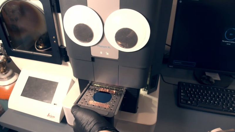
In e-beam lithography, or EBL, shapes are drawn onto a wafer using an electron beam in a vacuum chamber. This is a slow process compared to optical lithography, as used in mass production, but it is reasonably simple and very flexible. [Zach] decided to use his electron microscope as an e-beam litho machine; although not designed for lithography, it has the same basic components as a real EBL machine and can act as a substitute with a bit of software tweaking.
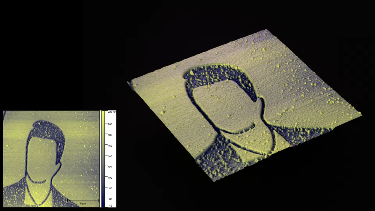
[Zach] explains the whole process in detail in his video, including how he tuned all the parameters like resist thickness, beam strength, exposure time and development time, as well as the software tricks needed to persuade the microscope to function as a litho machine. In his best runs he managed to draw lines with a width of about 100 nanometers, which is seriously impressive for such a relatively simple setup.
These e-beam lithography experiments follow on from [Zach]’s earlier research using lasers. Homebrew IC expert Sam Zeloof has also used electron beams in his work. Thanks for the tip, [smellsofbikes]!


I don’t understand. We used to do things like these during early 1980s at CEMI. Even back then it wasn’t really breakthrough science anymore.
Like CEMI in Poland?
At ETEC and Varian too. And Bell Labs before that. One difference is that the machines cost over a million and took up an entire room. Without knowing how good the mask to mask registration is, there’s no telling how useful this is.
Layer alignment is indeed important.
And honestly, layer alignment in semiconductor manufacturing is more impressive than the feature size itself. Since the alignment needs to be tighter than the features, else it will be hard to build anything reliably.
Yes, and now someone is doing it in their home shop.
He goes into detail about the history in the video, saying people have used SEM for EBL for as long as SEM have been around, and shows a ’79 paper on the subject. It is never purported to be new or bleeding edge.
Obviously lithography is a proven concept, every device that can view the video was made with it.
This is the intersection of ‘has Electron beam’ and ‘needs portrait of Johnny Bravo’.
Googly Eyes! XD XD
https://www.youtube.com/watch?v=zc7qJE9Nzo8
He says he has googly eyes on his cnc mill too and they’re way better coz it moves so fast. I sure hope we get a video some day.
I’d love to see if one could entrain a metal vapor axially with the beam for a 3d printer…
IBM tried this in the early 70s I believe. There is a strong coulomb force pushing electrons apart. It took huge magnets to force the beam to a point, but resolution is always a problem in microlithography. EUV is a softer name for x-ray lithography, achieving 13 nm resolution. That was the route taken instead of electron-beam lithography. This requires a set of sub-wavelength coated mirrors to soften the impact of the beam on the resist. These might need frequent replacement. The fabs using this equipment may be very costly to set up, control and operate. The economics of this approach for 5nm and smaller resolutions remains to be seen. There is also the challenge of fault-tolerant circuit design to deal with possible errors in transistor switches using only a few atoms. Creative solutions have emerged in generation after generation to deal with problems like these. Already innovative design, micropackaging, and other ideas are moving beyond just shrinking device sizes. Intel just discussed many of it’s futuristic concepts at the International Electron Devices Conference.